

In the previous article, I shared the initial steps toward creating an amateurial ASIC design. I had a concept for a colour generator, which I first prototyped directly on an FPGA. I also introduced some of the platforms and companies that make ASIC fabrication more accessible by allowing multiple users to share a single production run, TinyTapeout being one of the most notable examples. It’s a perfect setup for learning and experimentation!
In this part, I’ll summarize what I learned at the HDL level while transitioning from FPGA to ASIC, focusing on two of the most fundamental signals in any digital design: reset and clock. To fully understand the context, I recommend reading Part 1, which provides an overview of the project.
Design for ASIC: beginner’s lessons learned
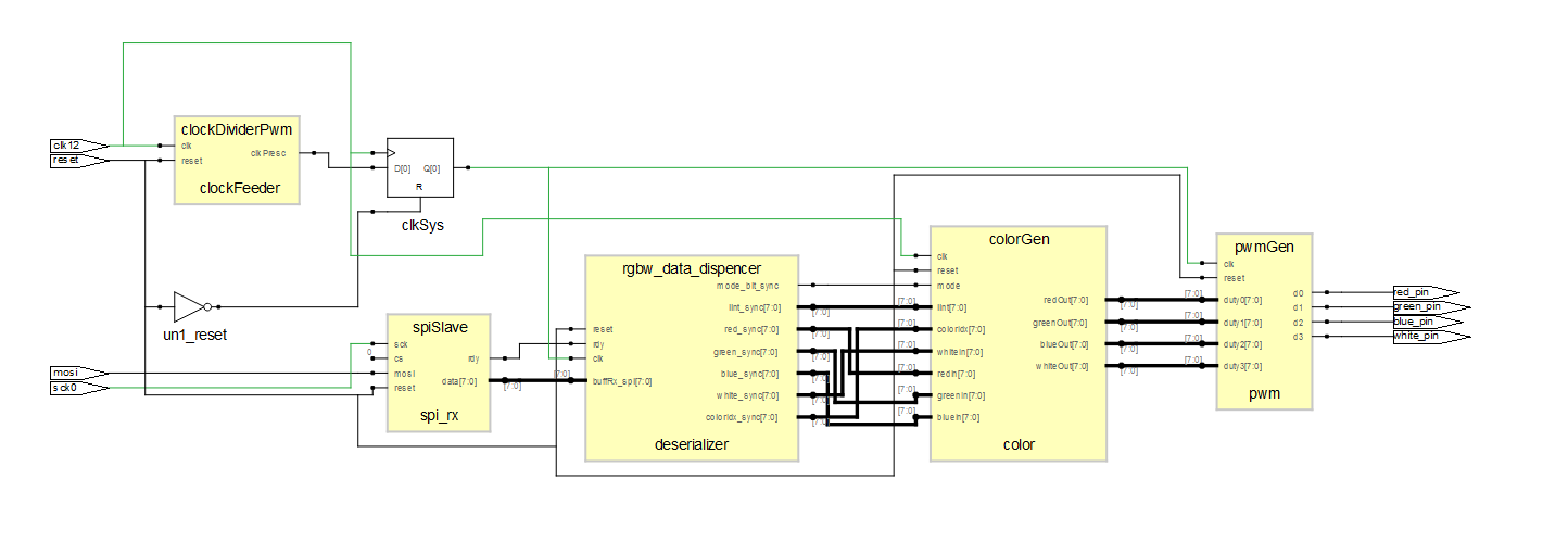
As anticipated in the previous article, the FPGA design was made in VHDL and roughly simulated in Aldec HDL, the free and ready to use tool back when I used the iCE40. It was shown the top level RTL, here for reference:
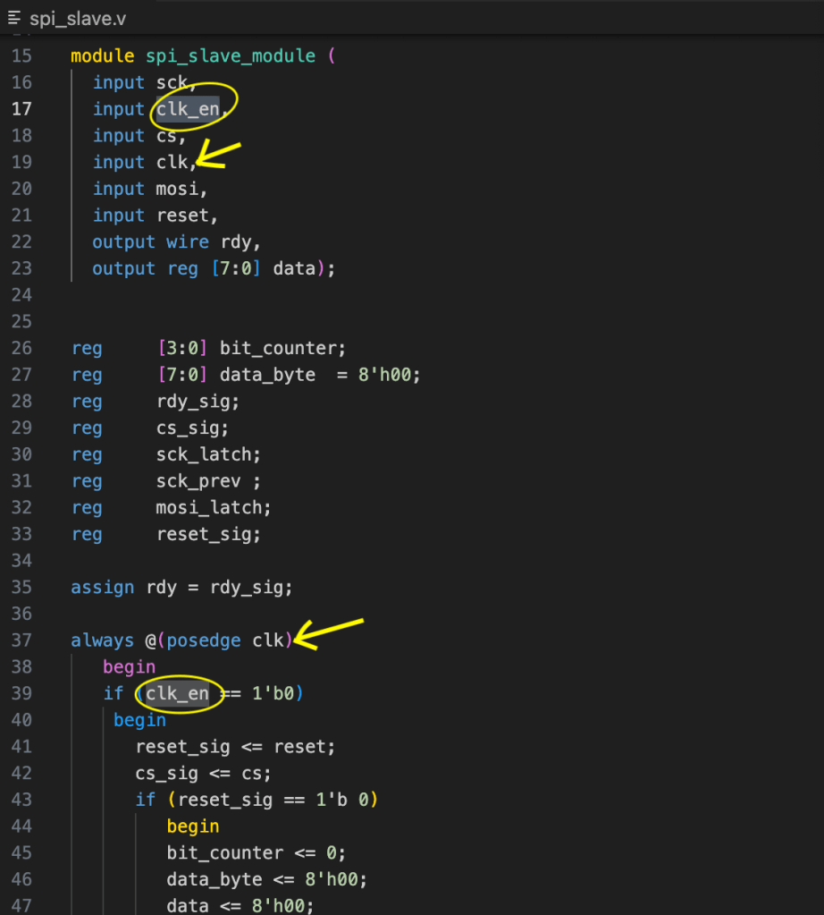
One of the first glitches I encountered was a fundamental issue: the SPI slave operated in a different clock domain, driven by the serial SPI clock. I had a basic synchronization mechanism, but in the end, it was much more easier correct to properly adjust the clocking scheme by feeding the SPI with the same system clock as well and then sampling the SPI clock:

Note that, since I have attached two outputs on a single PWM pin (right-hand side of Figure 2), the tool automatically added a buffer to maintain the correct fanout. For debugging, I performed manual waveform analysis, while the rest was tested directly on the board. I also added some ‘dbg‘ ports to bring out random signals I wanted to check each time. Now, let’s dive into the lessons learned I faced, when porting this design from running to an FPGA to be ASIC compatible.
Reset is not initialization
Figure 2 contains many RTL blocks designed for use with an FPGA. However, an FPGA is not just bare silicon; it is a complete IC that includes configuration memory, system RAM, clock management, I/Os, and hardwired SPI logic. When we synthesize an HDL description, the output is a binary configuration that defines the LUTs inside a programmable logic block, at least in the case of the iCE40 FPGA. This configuration specifies what values the LUTs should hold, which interconnection switches to close to connect different blocks, and more. As you can see, an FPGA has a rather complex block diagram, with a significant amount of hardware dedicated to initialization and signal distribution.

⏴ Figure 3 – Internal block diagram of the iCE40 FPGA
What we obtain after synthesizing the HDL description, is a binary file that, upon power-up, configures a complex system, such as the one illustrated in Figure 3. This figure highlights the fact that an FPGA includes a substantial amount of built-in hardware, with many components dedicated to initialization, configuration, and signal distribution – and reset control.
When working with an ASIC, on the other hand, you are designing everything from scratch, and there is no automatic initialization.
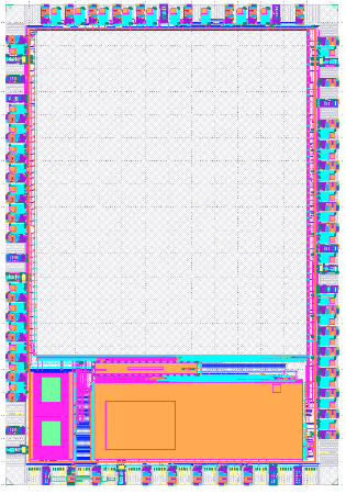
The lack of configuration support like in an FPGA can be “appreciated” in Figure 4 showing the Caravel SoC, where the empty space is nothing more than just raw silicon waiting to be filled with creativity.
Figure 4 ⏵
The empty silicon space of the Caravel SoC from eFabless
Back to the FPGA example, the code excerpt below, taken from the actual design initializes signals at “declaration”, exploiting the FPGA capacity to start the hardware in a given state (here signals at 0), and therefore having them initialized at such value even without going through a reset sequence:
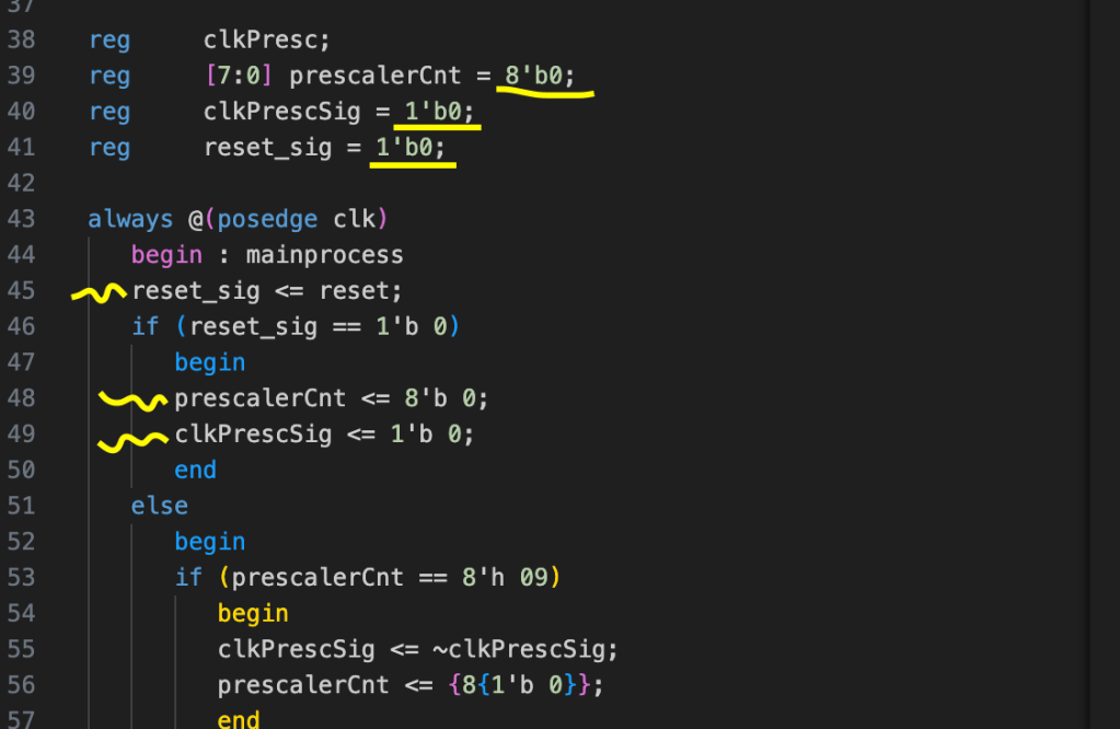
It is possible to use these initializations (underlined in yellow at line #39 to #41) for signals and registers to avoid routing a reset signal everywhere. This reduces congestion in FPGA routing by leveraging the initial values programmed in the bitstream, rather than implementing a traditional synchronous or asynchronous reset.
In fact, lines #48 and #49 of Figure 5 were not even necessary if the FPGA only needed to be reset at power-up only. However, in an ASIC, such initialization has no synthesizable meaning and everything must be explicitly handled within a reset statement. And so a synchronous reset sequence is fundamental.
A signal is not a clock
In RTL, a code snippet like the one in Figure 5 generates a block called ‘clockFeeder’ (see RTL in Figure 2), which produces a prescaled clock output. The FPGA tooling recognizes this as part of the clocking system and performs parasitic extractions and timing analysis specifically for the clock tree. In some cases, it even inserts additional buffers to support clock distribution within the FPGA.
As a result, in the timing report, both the primary clock and the prescaled clock are correctly identified and treated as clock signals. The key parameter that determines how a signal should be constrained (specifically as a clock) is the Synopsys Design Constraints (SDC) file.
The SDC file provides textual directives for the synthesizer and placement tools, using commands like set_output_delay -clock MyClock [etc.], or create_clock -period [etc.]. In the FPGA toolchain, this file can be at least partially edited, and in this case, both clock signals were already recognized, as shown in the outputs of Figures 6 and 6a:


Running a synthesis for an ASIC means generating a gate-level (GL) representation based on the PDK of the foundry that manufactures the IC. Unlike FPGA synthesis, this process is tightly constrained by the available standard cells and manufacturing rules. Here, an open-source toolchain called OpenLane is used, which includes various tools such as Yosys, OpenROAD, Magic, KLayout, etc, that can be installed locally. But for my design, I ran everything on the TinyTapeout remote server using GitHub Actions, which further limited the configurability of the SDC.
The result of this was that if a signal was not correctly recognized as a clock, it could lead to optimization issues. In one synthesis all was ok, but there were some warning of the type:
Warning: There are 356 unclocked register/latch pins. _3290_/CLK _3341_/CLK _3352_/CLK[...]Warning: There are 372 unconstrained endpoints. uio_oe[0] uio_oe[1] _3290_/D _3341_/D[...]As those were suspiciouly too many, I analyzed the waveforms locally using GKTWave, after having them generated by my test script running on GitHub. It was evident that the design was broken, with some signals not being driven at all:
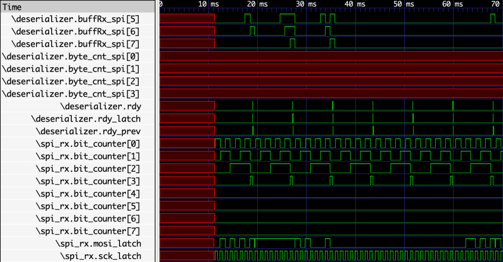
Through some debug it seemed that the byte_cnt_spi signal (but not only that one) was optimized away because the prescaled clock, derived from the main clock, was not recognized. Consequently, the logic was deemed inactive, and the byte counter was interpreted as never incrementing. In the of attempt to fix this, I redesigned the clock prescaler and clock distribution system.
A new clock system
Providing a divided clock in the sensitivity list of the unit won’t work or provide too many unconstraint and unclocked signals warning like shown before. Therefore the new approach supplies a clock pulse, with a period matching the prescaled clock, to all logic that requires it. However, now the SPI unit (like all the units), are also fed from the main clock. This main clock is used in the sensitivity list to trigger the logic that reads the clock pulse, effectively serving as a clock gate signal.
Additionally, since all resets are synchronous, I introduced a delay to ensure that all systems complete their reset using the scaled clock, before releasing a secondary, delayed, reset. Below a concept diagram of the implementation and the gate level waveform result:
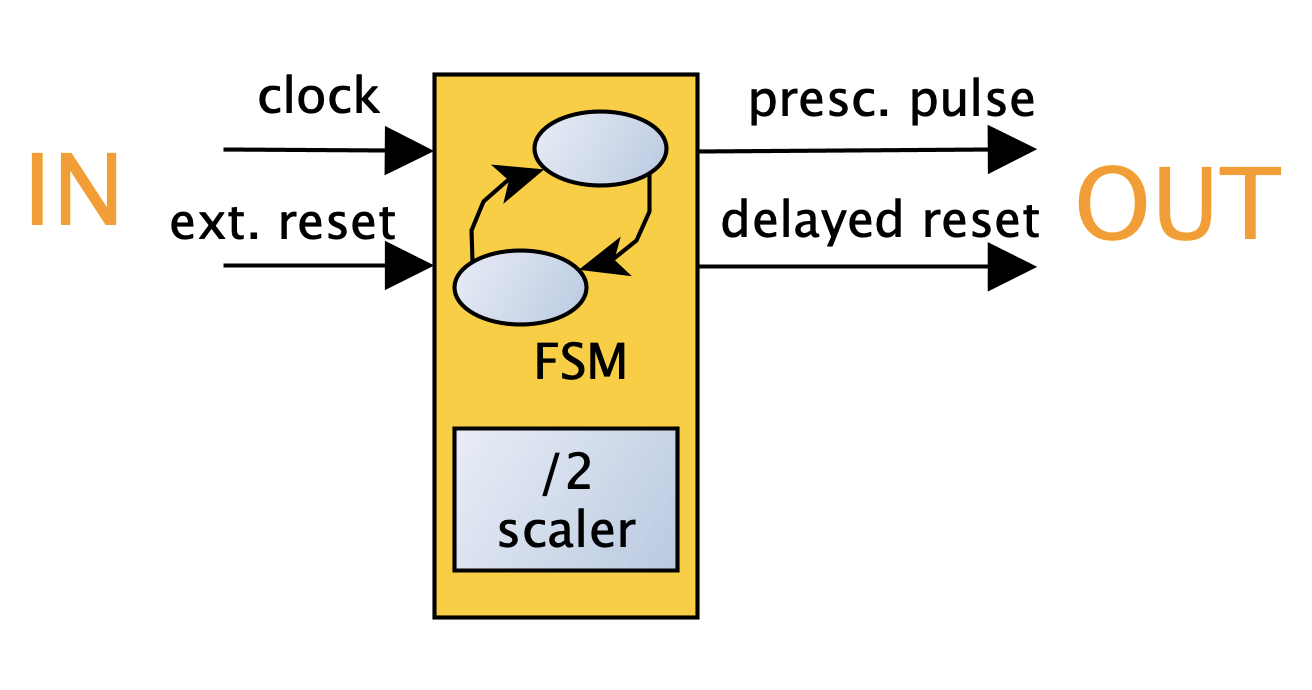
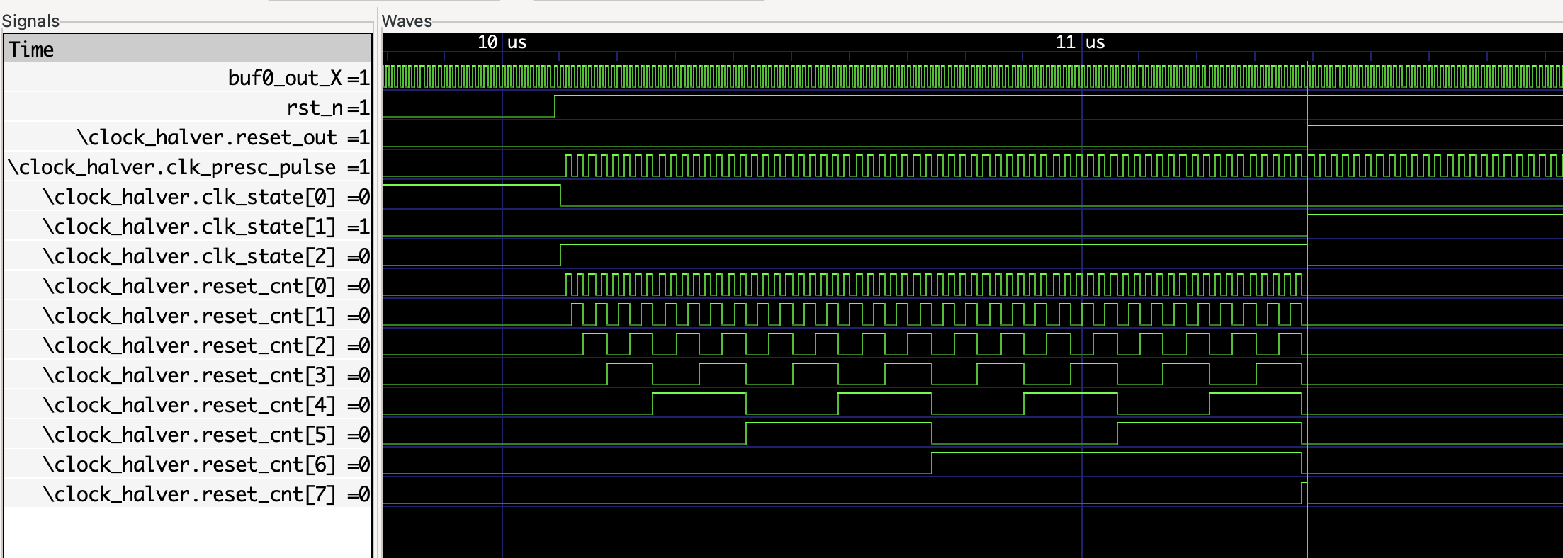
⏶ Figure 8 – Clock prescaler diagram and waveforms
Essentially, as soon the main active low reset (rst_n) is released high, the clock scaler outputs a scaled clock and creates a delay for a secondary reset (reset_out), keeping it asserted a given scaled clock cycles, here 128. This gives 128 cycles of the all units to fully reset, before becoming active, while having the main clock in their sensitivity list, which is used to sample the prescaled clock, here called clk_en:
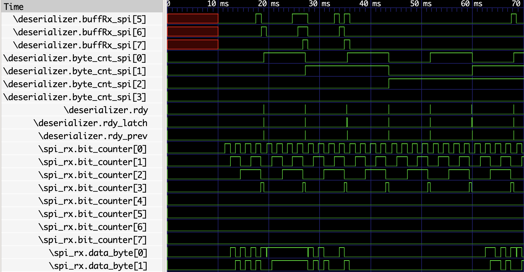
The result now is actually a fully functioning unit:
Next steps
Although the project was designed using a top-down approach, I found that exploring it from the bottom up helps ensure that, by the time we reach the top-level implementation, we also have a solid understanding of all the underlying components. Now that the basics such as reset, clock, and correct interconnection down to gate-level synthesis are under control, the next Part 3 will cover the lessons learned of the new units related to the main colour algorithm.

2 thoughts on “RGBW Controller ASIC, Part 2 – Design for silicon, clock and reset considerations”