
So far, I’ve documented the original FPGA-based project and the framework used to turn it into an actual Application Specific Integrated Circuit (ASIC), along with its functional description in Part 1. In Part 2, I covered a few key design considerations I learnt as a beginner when transitioning from FPGA to ASIC, specifically related to reset and clock handling, thinking it was nice to have them written down.
In this article, I’ll walk through another, and final conversion process, this time related to new implementations in the arithmetics needed by the Colour-wheel Processing Unit, also known as the CPU (random reference to a CPU absolutely intended, but it’ll be called CwPU to avoid confusion in the text). To begin to understand the reasons of the arithmetics, I’ll explain the core concept behind the processing unit algorithm, to finish by showing the whole logical architecture of the ASIC.
The main colour algorithm implementation
Prototyped in VHDL, the core part of the FPGA project is about generating four PWM signals to produce a colour in the RGB space from the HSB (Hue, Saturation, Brightness) colour model. For reference, check the “The colour concept” in the Part 1. The inputs for the HSB representation system are 3 values: the colour wheel index, which determines the hue, a scaling factor which determines the brightness, along with a white factor, determining the saturation.
The algorithm will “travel” in the HSV cylinder below, when the input are the 3 cylinder dimensions hue, brightness and saturation:

The “travelling” is done by the colour search algorithm, which traverses the entire colour spectrum by incrementally adding and subtracting the primary components starting from a default RGB value with no Saturation nor Brighness applied. Until the number of steps matches the specified colour index, it will continue the addition and subtraction. This progression starts from a pure primary additive colour (red, green, or blue), moves toward a midpoint where two primary colours are active (resulting in a complementary additive colour: cyan, magenta, or yellow), and includes all intermediate shades, with a step size defined by a constant ‘d‘.
Since the color index is an 8-bit value, and the full cycle is divided into six colour phases, each phase spans approximately 255 / 6 = 42.5 steps. In total, 255 steps are required to cycle through the full rainbow:

When going from a primary to a complementary, an increment on a primary colour value is performed. When going from a complementary to a primary, a decrement on a primary colour value is performed. At each step, a counter is compared against the colour index. Over 255 steps, the counter progresses through all six phases in order to increment as much as the index value. In the case of a full rotation (e.g. from phase A, red, to the end of the final phase F, red), all 255 steps are executed. This search of the “colour” is in reality just the hue.
Hue: overflow management in state machine
With an 8-bit index and 6 colour phases, we have 42 steps per colour, resulting in a total of 252 effective steps. This colour check can be sped up by incrementing ‘d‘, to have steps bigger than 1. When this is the case, it means we have to consider potential overflow, since the registers are 8-bit. The leftover steps can cause overshoots. For example, when transitioning from colour phase A to B, the RGB values might progress as {255, 0, 252}, then {255, 0, 258}, which means {255, 0, 3}, when using a step of 7 instead of 1. In other words, a visual glitch. To be conservative and being able to progress faster with coarser steps, also an overflow management is needed in case future tuning will be done in the incremental steps.
To check and exaggerate the overflow issue in order to simplify the overflow debug, here in Figure 2 it is shown the case with d = 7 (just because is 111 in binary and so is easy to see), done at lines #305 and #310:
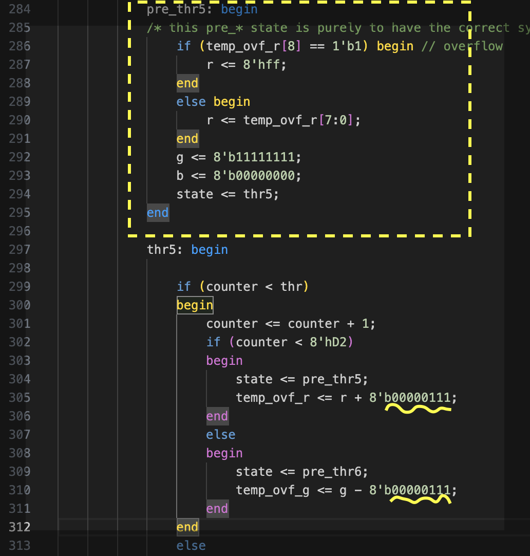
The overflow is checked in a “pre_” state, proceeding the colour phase state. Before executing the state THR5, the overflow of the previous THR4 is checked in a state called PRE_THR5, adjusting the values of the THR4 before computing the new numbers in the THR5. This is shown at line #284 in Figure 3. This state checks whether the previous colour value has its 9th bit set and manages the overflow before progressing to the next colour phase. Now is possible to implement the next step towards an RGB colour space, the brightness.
Brightness: designing a multiplier
Brightness is the amount of the hue we want to have. It can be linear, or with gamma corrections that follows a specific curve (usually to have a more “natural” transition for human eyes), and since it is about a proportional increment, the best implementation is a multiplication. The initial draft of a multiplier was done in few different ways. The first was an attempt to not use a real multiplication to save FPGA resources. It consisted of simply shifting bits to have a rough multiplications effect based on the brightness (lint_comp) value, as follows:
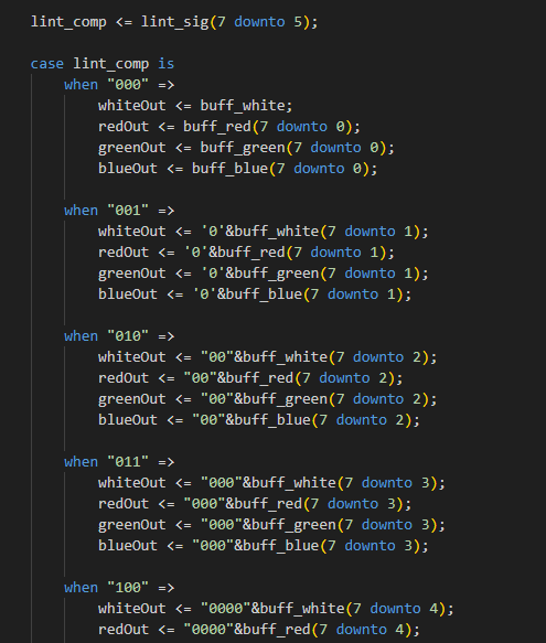
This approach is extremely stripped down, and it has a discretization over 8 levels only.
The second approach is a multiplication simply implemented with a multiplier operator. This would generate a multiplier from a default implementation that would occupy quite some resources of the FPGA/ASIC, also because I needed at least 4 of them. The effect would be quite smooth, but the expectation is that it would take quite some resources.
The shared multiplier
The final solution adopted is a sequential, shared, single multiplier. This would allow at least 4 clock cycles to complete 4 multiplications. But having a smaller combinatorial logic would also allow a faster clock speed, so effectively not necessarily increasing by 4x the execution time. I also gave priority in avoiding sync issues and keeping the signals output valid for 2 clock cycles, using a tiny state machine in the multiplier with a 2 clock tick latency, using a LOAD and READY signals to be used by the colour processor. A timing diagram is as follows:
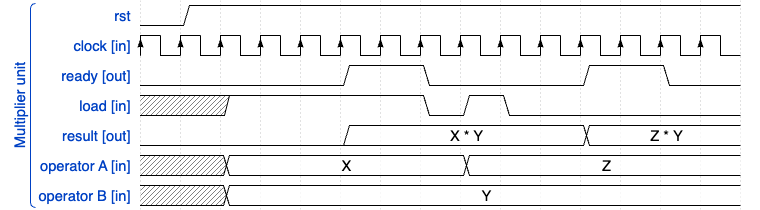
With a simulation snapshot of the gate level showing the interaction of the READY and LOAD and their timing confirming the functioning mechanism, showing how the colour processor requests the multiplication via the “ld” signal:

As anticipated, the READY (mult_ok) is made to be active for 2 clock cycles initially as I wanted to allow an eventual extra clock delay in checking the result when using this signal as a trigger to read back the multiplicator output register. In general, the processing of a single colour is still orders of magnitude faster than what is sent over SPI, hence the 2 clocks delay after the sampling point of the LOAD, is acceptable, and the main point was to prove to be able to save space via this shared approach.
The usage of the multiplier in the colour processor need only some logic for managing these signals, checking for the READY signal after propagating the values to the multiplier input registers “mult1” and “mult2”, and looping in this state as long as the multiplier output is not ready:
Multiplier’s silicon space, 4 dedicated multipliers versus a shared multiplier
run the test directly on the ASIC toolchain, since the optimization and synthesis would be completely different from the FPGA one, and I could not compare the resource usage since the FPGA does not uses standard cells, so I excluded that FPGA step.
Resource occupation comparison
The relative resource occupation of 4 synthesised multipliers without a shared one, in the hardened gate level design of the ASIC, has an increment of ~500 standard cells which is a +20% on a 2450 standard cells design. This leads to an increased routing by 7% on a 2-tiles silicon space (200 x 300 µm of silicon space, in this project).
While the use of a shared multiplier and the additional connections in the colour processors, there’s an increment of ~105 standard cells, which is a +4% only. This with a simple routing increase of 1.7% in the same 2-tiles space. Given the fact that having 4 sequential multiplication is still much more fast than an SPI transaction, this would not create issues on the colour generation latency.
Now after setting the hue and brightness, all is ready for the final adjustment, the saturation.
Saturation: implementing the white component
The last arithmetic implementation to fully convert the colour space was the application of the white component to the RGB channels, while also providing a separated 4th white channel by redirecting the Saturation factor to the white.
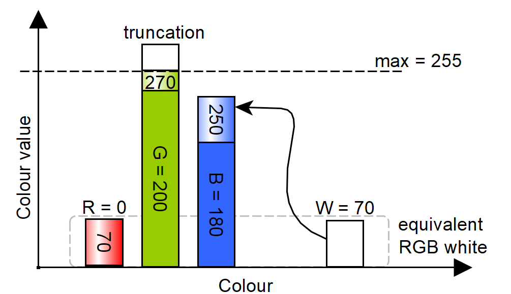
On the other hand, when saturation is minimal (i.e., maximum white), no distinct colour should be visible. This means all RGB components must be increased of an equal amount of the white up to complete desaturation. Having Figure 8 as a reference, the saturation starts from a given hue, by adding the white component to the RGB values, and if one of the primary colours reaches its maximum level, for example green, is then capped at 255 instead of the value it would reach after adding white (here 270), resulting in an equivalent RGB generated white of 70, along with a white channel value of 70. Red will also be 70 (which is the white+0), since in the hue it must remains zero because hue itself is made by no more than two primary colours, so if both blue and green are greater than zero, red must be zero as a starting point.
While the HDL implementation for this is trivial:

The final ASIC block diagram
This colour algorithm it is ecompassed in what is called a colour wheel processor unit (CwPU). This unit can be subdivided in different logic parts and can be conceptually schematised by the following diagram:
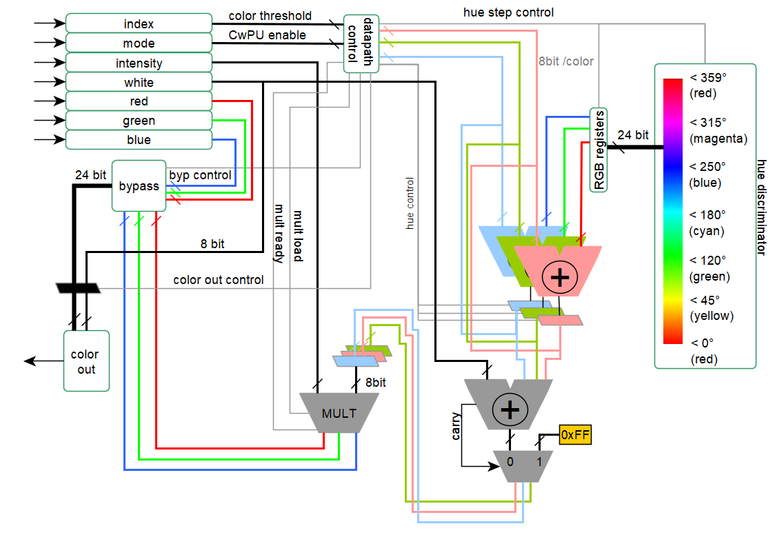
Focusing on the left side, it is possible to see all the registers used for the conversion of the colour space: index, mode, intensity, white, red, green, and blue.
The four colour channels can be individually output according to the mode command. In this case, none of the CwPU is used, and the whole ASIC effectively acts as an SPI-to-4-channel PWM converter. Conversely, changing the mode command will make the red, green, and blue signals to be completely ignored, and the CwPU is used instead, processing the colour index, intensity, and white.
As shown previously in Figure 2, the hue calculation follows a cyclic arithmetic progression, using three different (sequential) adders/subtractors, one per each primary colour. These compare the previous colour calculation with the current one. The “hue discriminator” in Figure 11 represents the FSM states of the colour progression. It holds the threshold values of the colour wheel, used to determine which and how long each colour component in the adders needs to be incremented, until the hue level index matches the colour index.
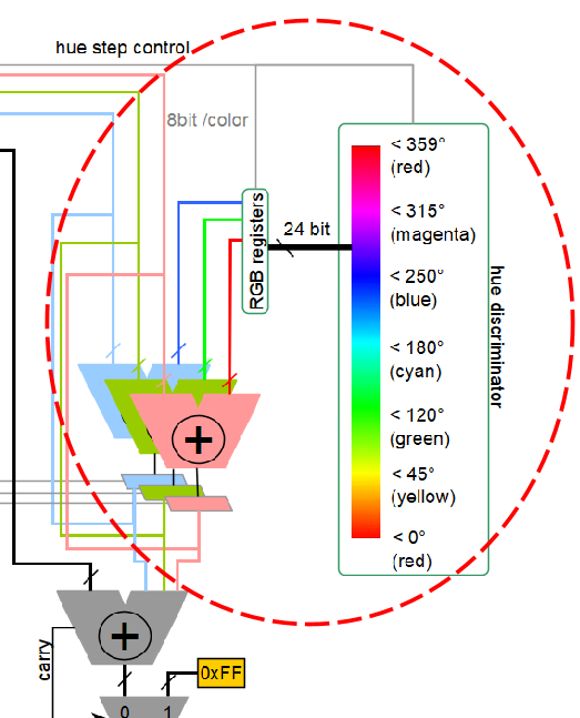
When the data is ready, it is latched to be used in a second adder with the white, in order to implement the saturation, capped at a maximum value of 0xFF, see Figure 12:
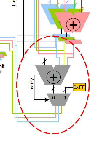
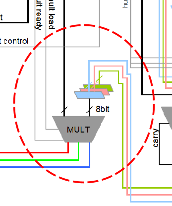
And only as a final step shown in Figure 13 it is made the multiplication for the brightness, using the shared multiplier:
And then the 24bit RGB colour space plus the 8bit white will be output to the PWM module.
Next steps
So far, we’ve covered the main steps needed to convert the FPGA HDL to an ASIC version, showing that the process isn’t as simple as a blind porting. ASIC development brings its own constraints, and in the final chip, there’s a lot that can go wrong. So if I will receive a non-functional silicon brick, I want to know exactly why.
To support this, several test stages are needed: starting with simulation, then lab testing. A simple “dumb debug” protocol, discussed in the next article, is implemented in the ASIC to expose internal signals, ideally even (and actually for) when things fail. Moreover, since the ASIC will be delivered with the official TinyTapeout TT08 development board, custom firmware will be required to generate signals and communicate with the chip. A custom RGBW output board will also be designed.
The next article(s) therefore will be more hands-on, no longer about HDL conversion, but about the hardware, firmware, and debug infrastructure. The goal is to provide a complete, system-level overview of how to test and use the chip effectively.


i think this is gonna be a powerful reference when microled era starts, its so exciting reading through these post (part 1-3) even though i didnt understand some of it, im so glad i found this blog from tinytapeout website, person like you that invent things and shares it (especially electronic circuit micro-architecture) is so rare. I cant wait for your custom tt asic hands-on blog. im quite surprised when i found out that the process took a year. Sam Zeloof needs to finish his first machine ASAP. Best wishes, blatantia.
LikeLiked by 1 person