

I initially had an idea to implement an RGBW LED color controller in hardware, but I only had access to an FPGA along with free tools (though not necessarily open-source). Later, while participating in the ETHZ Summer School in Zurich, I discovered how it’s possible, even for individual contributors, to affordably create an IC. At that moment, a mental (RGB) lamp switched on: what if I could turn my FPGA design into an ASIC? This journey turned out to be a rewarding learning experience, which I hope it could provide an additional reference for other curious minds messing around in digital design.
In this first article, I will introduce the project, outline the tools used, summarize what was initially prototyped on the FPGA, and briefly explain what made the transition to an ASIC feasible. Hopefully it should provide enough references for who is just starting to look around.
The initial idea and tools for FPGA
The design is a simple colour generator project, here is called RGBW controller, previously implemented in a FPGA, made with an SPI interface, and output to control coloured LEDs and logics in between. I had around an FPGA dev. board, the
The design is a simple colour generator project, referred to here as the RGBW controller. It was initially implemented on an FPGA, featuring an SPI interface and output logic to control coloured LEDs, with additional logic in between to generate a final colour. I used an FPGA development board I had on hand like the iCEstick Evaluation Kit and wrote the design in VHDL.

But just the board itself is useless if not supported on the software side, so let’s dwell into the tools adopted.
Free tools available for the FPGA design flow
The entire project was developed using iCEcube2 along with the Lattice LSE synthesizer, while Synplify Pro was used to visualize the RTL. Although Synplify is also a synthesizer (like LSE), it provides a more convenient interface for RTL inspection.
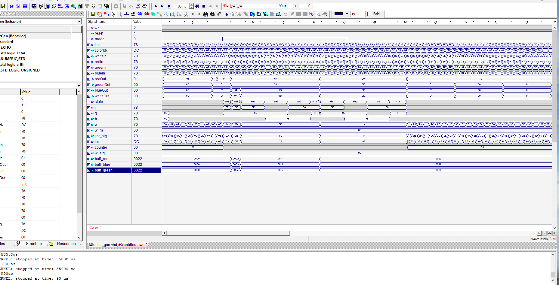
For simulation, the default toolchain did not include the classic ModelSim, but instead relied on the Aldec-HDL Simulator. This tool allowed for automatic testbench generation, including clock generation and input stimulus to trigger the internal logic. It was also design-aware, meaning it could display signal names and logic states in the waveform viewer as defined in the code, greatly simplifying the debugging of early-stage issues.
Below is a snapshot of the design running in Aldec:
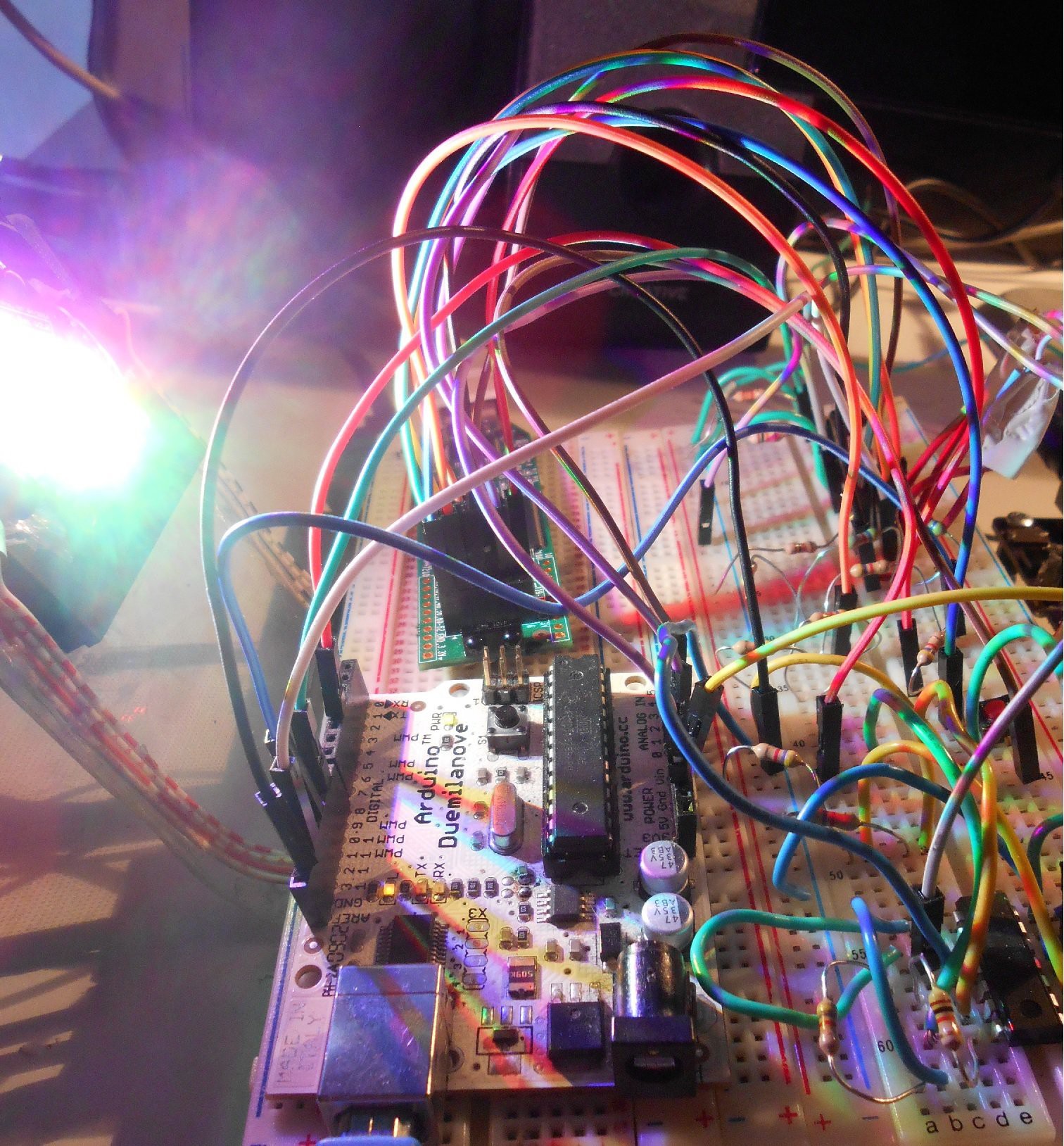
Once the main bugs were resolved on the simulation (i.e. the waveforms made sense), I began testing directly on the FPGA hardware. A test firmware running on an Arduino sent SPI packets and the PWM outputs were checked. The hardware setup was documented in a older Hackaday project: https://hackaday.io/project/19183-hardware-based-rgbw-lamp-controller.
In this article, however, I’ll focus on the high-level digital aspects of the FPGA design: its functional “requirements” (i.e. what the design does), a top-level block diagram, and the conceptual structure. These elements will serve as the foundation for the future ASIC implementation.
As anticipated, let’s see what was inside the FPGA to achieve this proof of concept.
The FPGA draft: a top down approach
The FPGA design was a port of a microcontroller-based project, which originally relied on standard microcontroller peripherals, that I now had to reimplement from scratch in the FPGA. These components, along with the core colour algorithm, can be divided into several distinct building blocks:
- A serial input interface (SPI): A simple and straightforward SPI slave, easy to implement.
- Data Deserializer / Register File: Responsible for handling incoming data, shifting it in, and latching it for processing.
- A colour-aware system: This forms the “original” IP of the design, being a system that can interpret and generate colour based on incoming data.
- PWM Module: A classic and simple digital-to-analog output, used to control LED brightness.
After this initial reasoning, before actually writing the modules, at the same time I quickly thought about connecting them, on a piace of paper. Incredible I still had it when writing this. Here, I realised a need for a complementary subsystem like a clock pre-scaler too.
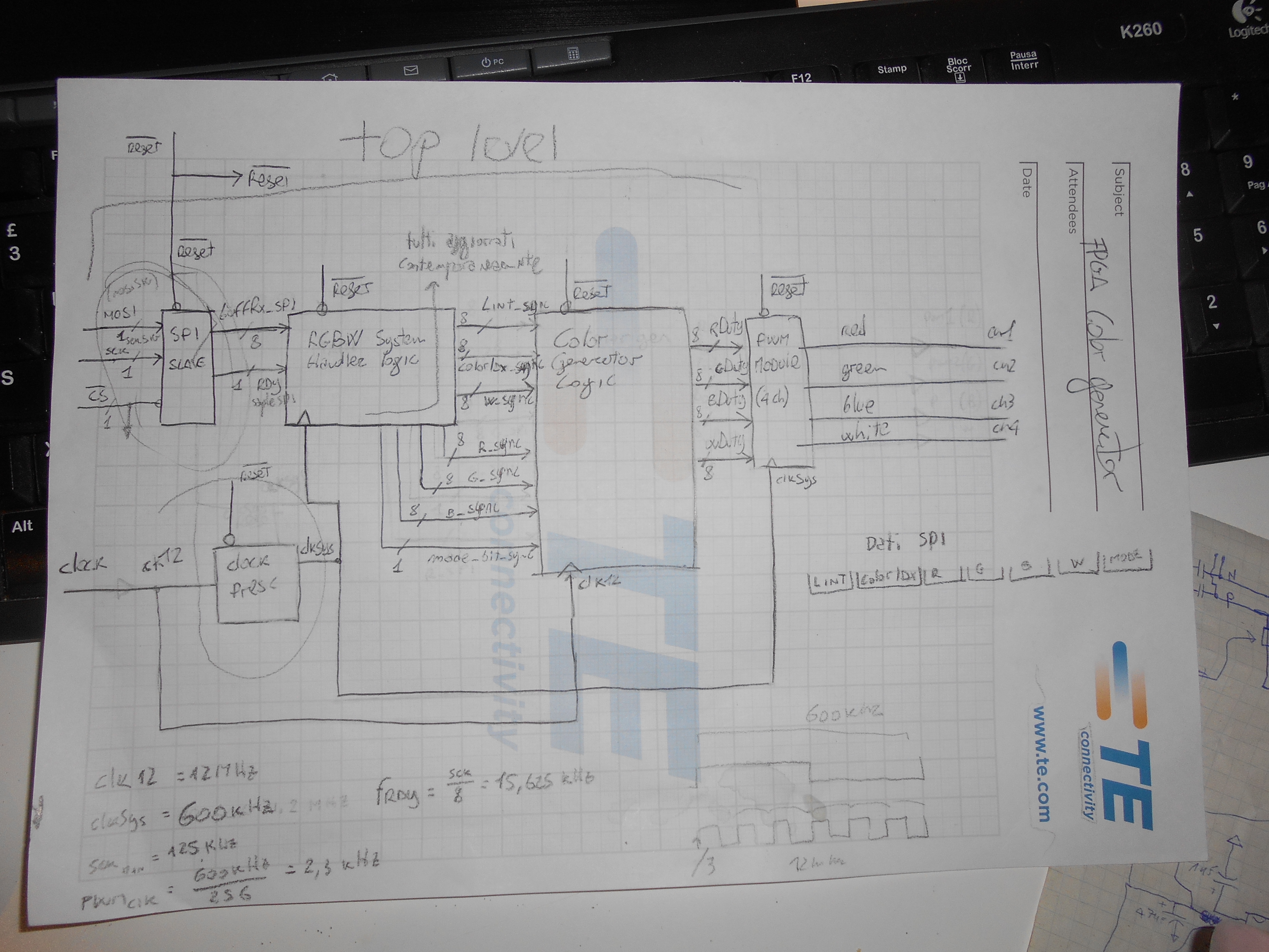
Figure 4 – The original top level sketch of the color controller
For fun, I compared the paper sketch with the final RTL, and surprisingly looked “close enough”:
The colour concept
The idea for the “IP”, the colour generator needed some further thinking. In fact is based on the convertion of the so called HSB/V (Hue, Saturation, Brightness/Value) colour space concept to RGB space, in order to create a colour with RGB LEDs:
colour = hue + saturation + brightness
This means that:
- The system needs a real-time colour generation algorithm based on an index or colour wheel, which required no memory and ideally no LUT (Look-Up Table), mostly for experimentation purposes.
- It must smoothly generate a colour tonality by adjusting the ratios of the primary colour LEDs (RGB): that’s the hue
- Controls the intensity of the white component, affecting how distinct or vivid the color appears: that’s the saturation
- Scaling the overall intensity of all LEDs: that’s the brightness
- …hence the IP will generate a colour!
The way a colour is affected by hue, saturation, and brightness can be visualized using the HSV cylinder model (or HSB, used interchangeably). Saturation corresponds to movement along the radial direction of the cylinder, brightness (or “value”) moves along its vertical axis, and hue determines the rotation angle around the cylinder.

There is also an additional consideration to make, regarding the saturation. In fact, white is generated via the RGBs primary components when activated simultaneously all 3 of them. This means is not a full-spectrum white and for this reason there is a need for a 4th PWM channel. This will outputs the white component, instead of using (only) the RGB simultaneously. In this way the colour rendering index (CRI) will be much higher, when a full-spectrum white LED is used on this channel.
Therefore the final requirements of the HW interfaces are just these IN and OUTs:
- 1x SPI slave interface input
- 4x PWM outputs
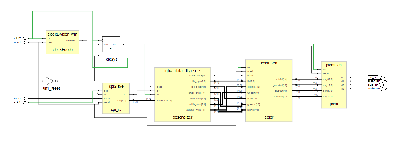
Below, I will include a (completely unnecessary) RTL representation of these blocks, just to provide a rough idea of their complexity, along with a brief description of each block.
The building blocks
clockDividerPwm: is a counter pre-scaling the clock for the rest of the system. Needed to slow down certain blocks and allow some testing with different clock speeds, especially at the beginning of the implementation.

spiSlave: a shift-in register with a state machine counting the bits and dividing them in bytes, with a byte sync signal. Complexity here came from the synthesized state machine and the preamble symbol discrimination. Thata is propagated to the next block, the rgbw_data_dispencer.
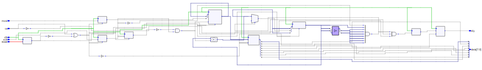
rgbw_data_dispencer: this was originally intended to be the main logic of the design. In the end, it simply handles the data received from SPI by checking for a sync character, counting the subsequent characters, and storing the values in a register file. The register file is updated at the end of each complete SPI transaction, all at once, to ensure consistent behavior. There are a total of seven registers that are latched from the SPI interface, and these are then passed to the colorGen block.
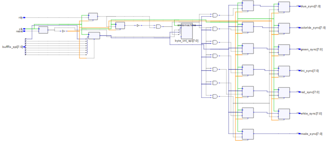
colorGen: this is the main logic, implementing the convertion from the HSB colour space to the RGB(W) one. This blocks makes sums, multiplications and have states machines, making it the most complex part of the project. The output is just the RGBW 8 bit values ready for the 4 channel PWM modulator. I won’t even try to comment the RTL, but on the left are the parallel inputs latched from the data dispencer, and on the right-side the 4 8bit registers for the PWM channels to be fed to the pwmGen.

pwmGen: is the PWM modulator, essentially a counter with 4 comparators taking as input the 4 8bit values of the 4 colours, now in the RGB(W) space. Its outputs are directly connected to the IOs of the FPGA, which can be used to drive 4 RGBW LEDs.

The SPI protocol
SPI slave is Mode 0 as shown in this timing diagram, highlighting the preable and first byte transfer:
Rather than viewing it bit by bit, when zooming out to the byte level on the SPI bus, the entire packet must conform to the following structure:
Note how there are 7 values, as much as the register file registers, except the sync symbol/preamble (only used by the SPI slave subsystem). Here the ranges supported by each of the value:
- preamble: 0x55
- intensity: 0x00 – 0xFF
- color index: 0x00 – 0xFF
- red: 0x00 – 0xFF
- green: 0x00 – 0xFF
- blue: 0x00 – 0xFF
- white: 0x00 – 0xFF
- bypass mode: 0xA4 for the color generation, 0x21 bypass
With bypass mode to 0xA4, the RGB values are ignored and the colour processor is effectively engaged and active, performing teh HSB to RGB convertion as following:
- The Color Index will be used to generate the RGB hue
- Converting the white to an equivalent RGB value to implement the saturation, summed to the already generated RGB, up to maximum white, or minimum saturation. Example: W=240, RGB = {32, 4, 128}, then RGB+W={255, 244, 255}+{240}
- Brightness will be mapped in hardware to convert 0-255 of intensity in a 0 to 100% equivalent fixed point multiplication factor to the RGBW values.
With bypass mode to 0x21, the RGBW values are directly replicated on the PWM outputs, and multiplied with the intensity. Because there is missing the colour elaboration, the latency will be much lower, making it effectively an SPI to 4 channels, 8-bit PWM converter.
Moving to ASIC
Now that the design requirements have been explained, I’ll briefly mention how it’s actually possible to deliver an ASIC, in practical terms. The detailed implementation steps and the challenges encountered while porting the design to ASIC will be covered in the next article.
As mentioned in the introduction, I participated in a one-week workshop at ETH Zurich focused on open-source ASIC design and microprocessors. During the workshop, I became more familiar with the TinyTapeout project and its community, as well as with several experts and researchers in the field of IC design and open-source tools.
A bit of background
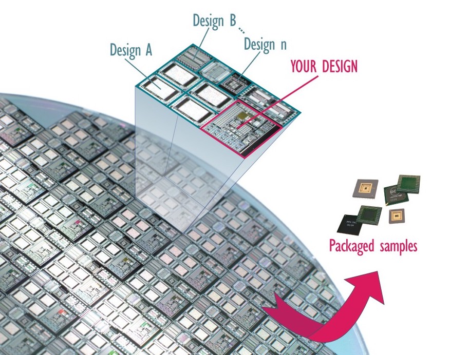
TinyTapeout is a project aimed at reducing the cost of manufacturing an ASIC in silicon. Without them, to make an IC, universities and smaller entities lower the cost by joining an MPW (Multi-Project Wafer), where the cost of a single wafer is divided among different clients, similar to how a low-cost PCB manufacturer operates. Here, the cost is still in the 10k USD ballpark per customers, and per production run.
The TinyTapeout (TT) project took the Caravel SoC from eFabless. The Caravel has a Risc-V controller to handle the GPIOs and power, but the rest is left free for the user adopting this design:

TT developed, in the blank empty area, “lanes” used to host “tiles”, each of them implementing a tiny, different design from the community. TT also designed a system to address each tile, which will be exposed to the Risc-V interface, which will route the tile IOs to the chip GPIOs.
In figure 12 an example of a 4th tape-out, or tt04, where can be seen the user tile, containing a single, self contained design which is shared among all the other people submitting their designs in the other tiles. Here, the empty space without tiles can be seen, showing only unrouted, “yellow” metal layer:

The tapeout I contributed to, TinyTapeout 8 (tt08), used an improved architecture called OpenFrame, created by eFabless. This version does not include the RISC-V control system, which makes more space available for user designs, up to 15 square millimeters. Within this area, TinyTapeout was able to integrate 512 individual tiles by using an improved addressing system that replaces the need for a RISC-V controller. For a user like me, this resulted in a theoretical 512 times cost reduction, although the actual savings are slightly lower because they include TinyTapeout’s operational margin.
Here a snapshot of the tt08 GDS layout also with the RGBW design highlighted (documentation here, and details are described in these articles series). Is possible to also all of the other designs, viewable at tt08 page. Notice how also this is not fully populated, and it doesn’t have the additional RISC-V controller:

Notice the control logic in the center, made by TT. And on the left, my design which occupies 2 tiles, with an astonishing area of 160×200 um.
But now let’s see the design flow leading to the ASIC made with the 2 tiles, starting from the tools available, used by a profane like myself.
The open-source tools for the ASIC flow
The tools available for the ASIC were the one under the umbrella of the OpenLane flow implemented by eFabless. In my case I was interested to know which tools makes the actual RTL synthesis and how: Yosis. It seems these are working best with Verilog. As the original version in FPGA was made in VHDL, before using those tools, a convertion was needed. Converting into Verilog can be done via ghdl. But the conversion is quite ugly, losing the variable names and supporting only a subset of statements.
So I needed to use another tool V2V SynaptiCAD, with a mixture of ChatGPT and manual work to check the algorithms and integrate all together. After that, not only I know Verilog now, but I needed to have all working with the FPGA, therefore it was run thought a regression test in the iCEcube2 with the tools used for the FPGA flow.
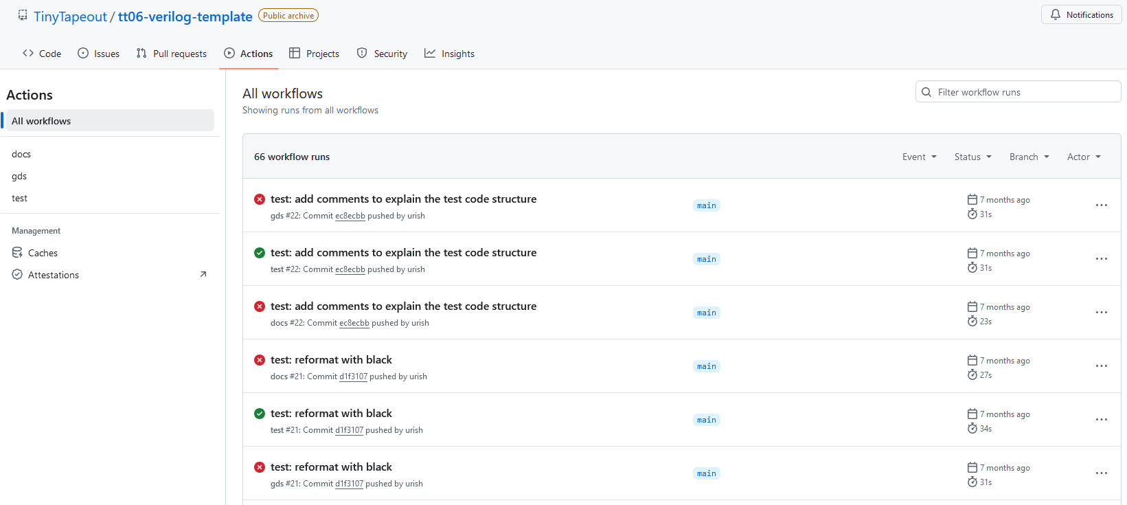
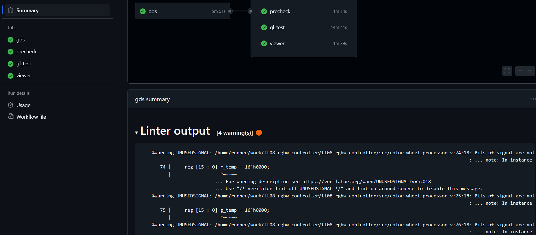
Now, we have couple of options: either installing the OpenLane software locally, or using the TT provided template which runs the preconfigured GitHub Actions. Below an excerpt of how the Actions looked like based on how were setup by Tiny Tapeout: a run for the GDS compilation, the documentation and the test.
So to have the tests running, I will need to write a proper testbench, this time via cocotb and assertions (or writing the Verilog testbench from scratch), coupled with GTKView. The simulation will be run locally on my PC with Icarus Verilog, as well as the RTL compilation, allowing to make changes and check them on the spot. For the actual synthesis at gate level (GL synthesis), I either needed to install OpenLane or run the Actions. For semplicity I decided to base my self on the Actions:
If one never did that it feels a bit alien, but in reality is very easy especially following the guides on the template itself: comply with the template will normally guarantee to comply with the flow.
Conclusion
At this point we are ready to begin the journey in the convertion of the FPGA HDL design into an ASIC complatible one, worth an article on its own. In the Part 2 I will discuss through the design changes I needed to make in order to comply with an ASIC design, starting from the clocking system adventure.

2 thoughts on “RGBW Controller ASIC, part 1 – An FPGA design forged into an ASIC”