This is kind of a report of the second attempt in making a power constant current source, high speed, for power LEDs. Taken all the errors made previously, I tried a new linear based current source which should be kept “simple” and “fast”.
Technology adopted so far
I have experimented with power LEDs, how they work and various solutions possible to drive them. With a pseudo evaluation board I tried the very inefficient linear based approach, with the intent of making an high speed driver. As you can read in the previous article there are some troubles that make this kind of circuit everything but not so straight for a rapid DIY approach. On the other side, this journey was very educational to me. The current absorbed per LED (700mA), thermal dimensioning and the LED descriptions are still present in the previous board description, while here I am focused on describing the improvements in this version.
Troubles with the maximum input voltage, offset, mechanical handling and power efficiency have been encoutered and herein somehow fixed with a “new” version. Moreover, I perfectly know that there is still no input and short circuit protection, as long as various improvements that can be made. But was only the beginning of PCB design, with PTH (plated-through hole), which occupy space and size, so costs. So I said: do not put any capacitor, what could happen? Yeeah, herein I will describe how this choice was something comparable to only an evil genius would do.
Troubleshooting the offset
The main issue on the first version, was related to the offset introduced by the op-amps. Therefore, I need to countermeasure this by injecting some current in the sense resistor. This will lead to some dummy current absorbed by the device, thus the capability to deactivate this functionality. This can be accomplished by using SMD transistors and the proper resistors to inject up to: 


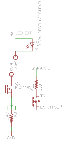
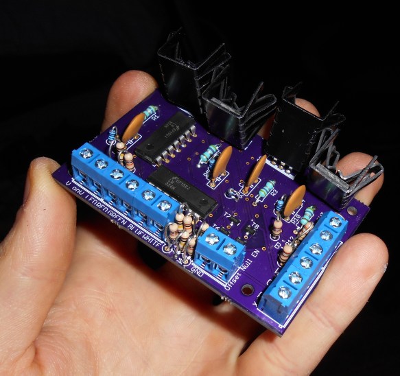
This compensation will lit up the LED a bit lower, since part of the current used forthe compensation will not flow though the LED, but it is not significant on the final test. I have actually used some 330Ω and the result is achieved equally. But at the highest defined voltage here will source up to 20mA, meaning the the regulator will attemp to flow 20mA less in the LED. In picture below, R11 and T6 are the current limiting resistance and the signal MOSFET used to let deactivate this offset compensation, while Q3 is the main MOSFET which source current for the LED. The X6-4 and X5-4 are the connectors of the main board and the “satellite” which mounts the LEDs.
Troubleshooting input voltage range and voltage dropout
Another issue was related to the high value of the sense resistor. This high value was chosen in order to make the system more stable, since the output resistance of the op-amp combine with the MOSFET capacitance, will add a pole. The circuit will be stable if the frequency of the added pole is more than a decade above the circuit’s bandwidth. But I DON’T know the output resistance of the op-amp. Empirically, increasing the efficiency on the sense resistor by reducing the resistor’s value itself and the input voltage, lead to a greater ringing, because reduces the pole frequency. Thus, the system must be slowered down with respect the expectations.
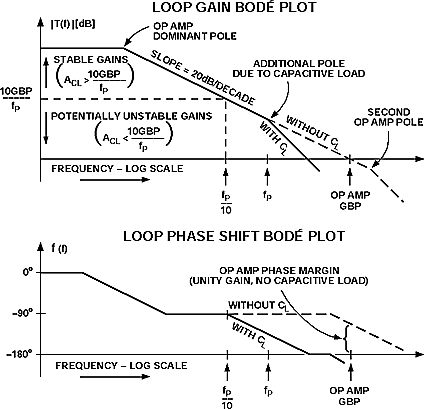
As can be seen in the picture above, the capacitive load (here the main MOSFET) introduces a 


Reducing the input voltage, will bring to the need of reducing also the input control voltage. This reduction has been made by 10 times, so in the board also the voltage divider resistors have been added. Then a buffer placed before this voltage reducer allowing me to not interfere with the resistance divider factor. Reducing the voltage drop on the sense resistor, allow me to power the system with a lot power savings which is not wasted anymore in sensing the current.
The main pain in the amp was to choose a different MOSFET that has a lower theshold voltage, allowing me also to use a lower voltage on the opamp. The choice was on the IRLI630GPbF. Almost 2V of threshold, but big input capacitance. Below the entire schematic:

Handling and manufacturing
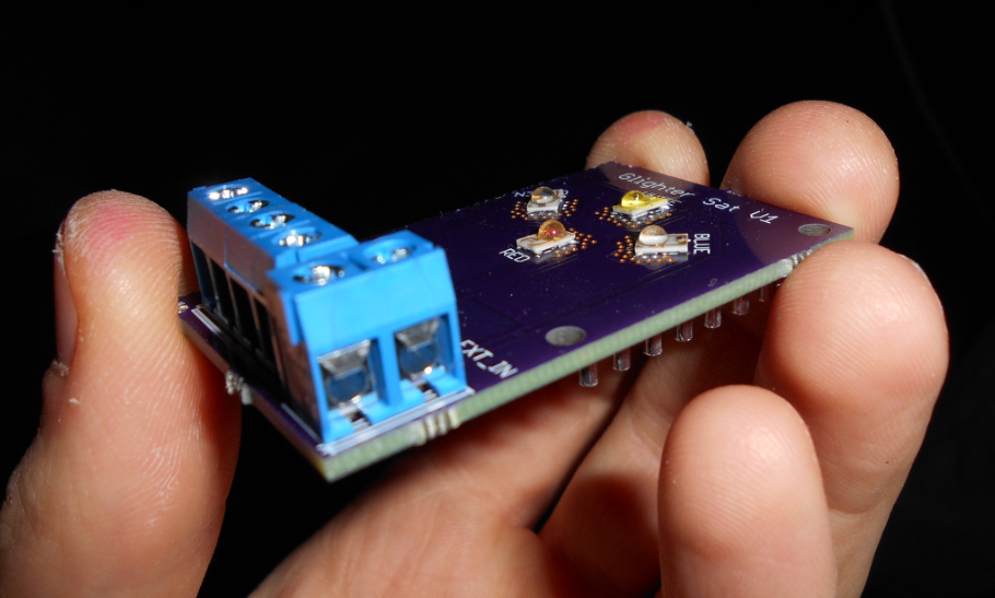
I preferred to desing also a separated satellite PCB which is used to store the LEDs. I wanted to try to make it more compact. In these pictures are shown the main board and the satellite, sent togheter to OSH Park as a single design. In terms of cost, that was not a good idea. I like to call it experience.

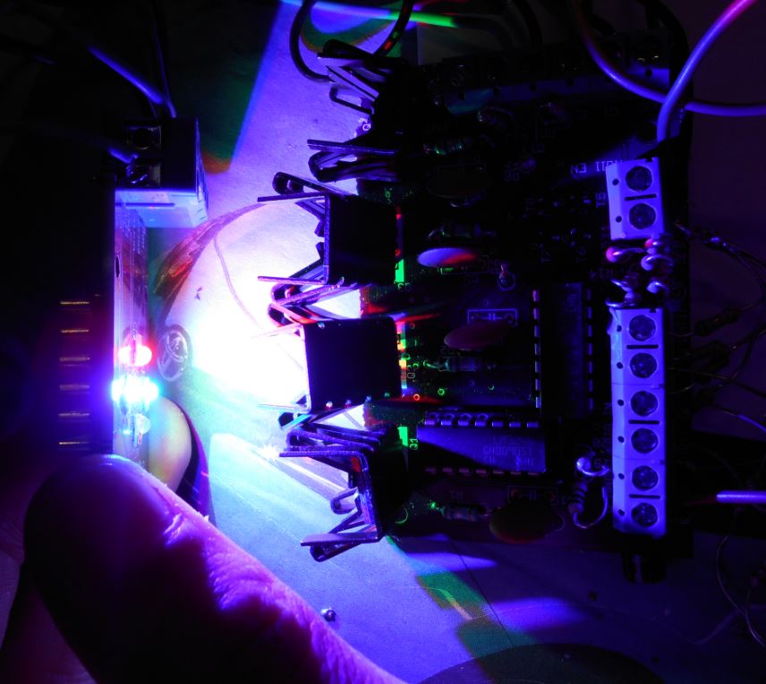
Here the final assembly:
Frequency troubleshooting and considerations
The oscillation was even worse, despite the compensation. That’s the evil genius’ choice. I didn’t put any filtering/bulk/tank capacitors. Putting a 100uF one on the main voltage rails, eliminate the oscillation. This let me understand that in my setup I had a lot of wires that are going from the board to the power supply, keyword: RLC oscillator.
At first, I thought to make a pole-zero compensation, but that requires knowledge of the output resistance of the op-amp. Therefore, the practical approach was to understand what was going on. Since the MOSFET is a capacitance in series with the op-amp, will likely make an high-pass filter, putting high frequency noise to the feedback loop. A capacitor in the inner-loop at the same (-) terminal of the op-amp would actually compensate for this.
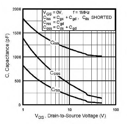
But lowering the voltage will trigger again ringing. The answer is in this picture:Reducing the supply voltage to 3.5V will increase the (already fat in its own) input capacitance, Ciss and also the output capacitances of the MOSFET. By speculating, I assuem that this reduces the pole frequency combined with the output resistance of the op-amp, while putting even more noise with higher magnitues at the feedback.
And here the LEDs powered with a stable conditions. As always, if you think there are errors or suggestions, feel free to comment or contact me.