
It was not long time ago in which was developed a small DC-DC LED driver – Glighter-S, my first switching LED driver. It was the natural consequence of the need for efficiency after the development experiment of the linear LED driver – Glighter. No long time after these experiments, the need for analog control in a equivalent (i.e. same build cost, same appearance or usabilty) solution was needed. And most importantly, I wanted to learn.
The outcome of this experiment is also available on Tindie on a tested board, for who is interested- otherwise, keep reading!
Searching for parts
The ideal solution would be find something related to a cheap LED driver. The selection went quickly down to a converter topology already cheap by definition, given its simple control circuitry. And simplicity often means also robustness.
And here they are, the hysteretic converters. In the end, do we really need a constant voltage power supply, which adjust its output according to a shunt measurement? Why not just exploit the fact that the inductor adjust its voltage to keep the current “constant”? Like the usual 
These converters are using a Schmitt trigger comparator, a voltage reference and an output driver. That’s it. Let’s see to the part used, the ILD4001. I’ll take the same example from a previous article:
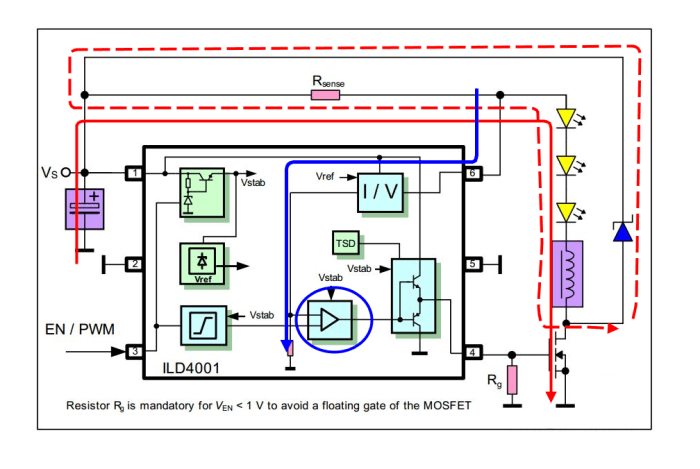
The dashed arrows shows the current path when the inductor cannot let flow current to ground (MOSFET open). It gets a continuous flow through the blue diode, which continues to power up the LEDs and provide a shunt voltage, read back trough the pin 6 (with the blue arrow). Through an internal transconductance amplifier, will generate a current proportional to the shunt voltage, which will generate a voltage through an internal resistor, for the comparator (in the blue circle). When the shunt voltage reading gets lower, the inductor start to decrease it’s current, so the comparator turns on again the MOSFET, the current raise to a certain value and the cycle repeats.
This part, like many of its category, is able to adjust the internal reference to support analog control as well, on the same pin. In this case, any voltage within 0.6V and 2.5V allow analog regulation. A PWM signal can either modulate the analog signal allowing mixed contrast ratio (see here for a dedicated article about that), or going from 0V up to supply voltage safely, squaring the output between ideal no current and output set maximum constant current.
Among other parameters, the switching characteristics table shows the key ones:
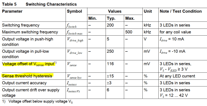
Highlighted in yellow, the voltage offset internally predefined, imposes the amount of drop on the sense resistor, hence the maximum current in which the system ideally settle:

But to let the circuit act with some control, this offset needs an hysteresis, here set to 
So its already clear that this cannot provide a very precise current, by definition. Either, the frequency will be totally dependent on the speed of charge and discharge of the inductor. Give up? This can be solved.
Switching frequencies and uncertainties
Also, the frequency is not constant, as will depends on the drop of the LED, the slopes of the current in the inductor and as a consequence, the supply voltage. In this article I wrote about the rising and falling slope of an inductor, trying to figuring out what happens to the average output if the PWM control signal is much faster than these slopes.
But now let’s assume there is not PWM control, but only full on. In this case, the driver will settle to a steady state, bumping the output 15% up and down, respectively. So assume now the following situation:
- LED Vf = 2.8 V
- Rsense = 0.3 Ω
- Input capacitor of 2.2 µF
- L = 68 µH
- Vs = 12 V
- Vdiode = 0.25 V
The LED voltage is that one is because I am testing with a LED which is a Luxeon Rebel LED with approx. 2.8V at a current of:
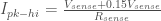
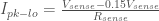
and according to equations (2) and (3), the peak levels are:
The input capacitor is to reduce noise on the input, and a ceramic one of 2.2uF seems to work fine, giving reasonably stable supply to the chip. While the 68uH come from a central value suggested in the datasheet, proving itself a good value to not saturate at such current and switching frequency. But wait, we don’t know it yet!
So, here the output current at steady state taken from the Application Note of the ILD4001, edited here with my current:
The time of the rise slope goes from the lower peak to the higher and viceversa, and the frequency is the inverse of the sum of such durations. The delta is just:

Therefore the rising slope is:
and the falling slope is a bit longer as there is no energy in the game but the one stored in the inductor, slowing down the process, while the diode here contributes to absorb the energy:

The switching frequency is therefore dependent basically in a linear way on every single parameter:
Stealing the ripple from the LED
At least, is still possible to reduce the ripple. Here the intention is to use a constant current. A current which is shaped like in Figure 3, does not allow a constant current, specially if the LED light needs to be measured by some sensor, this ripple will get detected. Therefore, taking the example from the datasheet of the LM3404, the possible solution may rely on convey the AC component into a parallel capacitor:

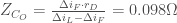
So the impedance of the branch with the capacitor is:

The filtered current, is… filtered, because of the current divider principle:
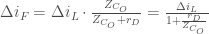
Now the only knob adjustable is the capacitance and from (9), the bigger that is, the smaller the 


Let’s pick couple of values aroud the center current, but close enough to linearize around that point with no much error, for example, 300mA and 400mA. Therefore:

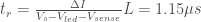
Now the original ripple current is 30% of the total current (corresponding to 0.3 times of 386 mA, so 


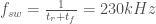
Because eq. (8), to have a ripple lower than this 5%, with a switching frequency of 230kHz, the capacitance must be:

The hardware and the results
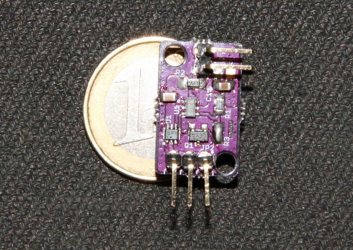
The boards were designed to be very small and have a similar feel of the Glighter-S. Here how they look like:
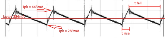
Probing the voltage difference across R2 (in figure 6), allows to see the current, just like Infineon did for Figure 3, here on my scope:

Looking at the purple trace on the top, the real frequency is 316 kHz, with

The theorethical frequency was 230kHz, but given the supply, the inductor and the sense uncertainties, combine with the LED parameters approximations, the result could be considered within the same ballpark. Also, the 
What about the LED current?
To measure the LED reliably, due to the I/V curve approximation, measuring its differential voltage may be too far off the reality because is not linear with the current! A precise approach would be either:
- Measure with a sense resistor in series with the LED(s), given that the resistor is overall way lower than the overall LED(s) dynamic resistance. This may be complicated but doable.
- Extract with calculations the current capacitor, since $latex I = C \frac{dV}{dt} $, basically consisting in multiplying the slope of the V/s by the capacitance and subtract it from the overall current, but with this an indirect measurement and you can just assume and never really measure.
In the end I decided to measure directly the luminous “flux”, because around that current value, a the flux curve is pretty linear. Because it is linear and I need to measure the ratio of the illumination ripple before and after the capacitor, it should be fine for a qualitative measurement using the ratio of these two measures.
I used an OPT101 with a feedback resistor of 500kΩ, meaning the sensor has a bandwidth aroud 30kHz, an order of magnitude lower that the switching frequency of the ripple. The output signal is expected to the quite low, but measurable. The schematic of the sensor setup is just this one:

The output with no filtering capacitor shows a clear ripple on the received light at the switching frequency:

Going step by step, a 2.2uF already make an effect:

Trying with a 6.6uF (3x 2.2uF) which is close to the estimated 7uF, will provide this:

The theoretical reduction is supposed to be from 30% of 386mA to its 5%, i.e. 19mA. This reduction from 153mA to 19mA corresponds to a factor of 8. From the results of the sensor, the reduction from a real 150mA (and not 153mA) should be proportional to the reduction of the ripple taken out from the OPT101. Between Figure 9 and 11, the reduction is at least 3 times. Theoretically, with 6.6uF, running through the eq. (11) and (12) again, the reduction should be around 5 times.
Conclusions
Considering the uncertainties of the capacitors, the LED tolerance and the noise on the emasurement, for a qualitative measurement this result shows the effectiveness of the filtering solution and also that the calculations are giving a good estimation for a filtering capacitor. I tried the board also up to currents of 700mA, mistreating it ecc, the chip never broke. So all this effort was worth a working board, compatbile with 90% of my LED projects ideas.
