One of few repairs that went smooth and succesful. Using a monitor with integrated USB hub can be useful, but also tricky, if such hubs are designed in a cheap way or is not fool proof, and I am a fool. If that is the case, overloading the output lead to a dead port. And it is exactly what happened.
Opening the monitor
The monitor is the AOC I2475PXQU, here are its USB ports:
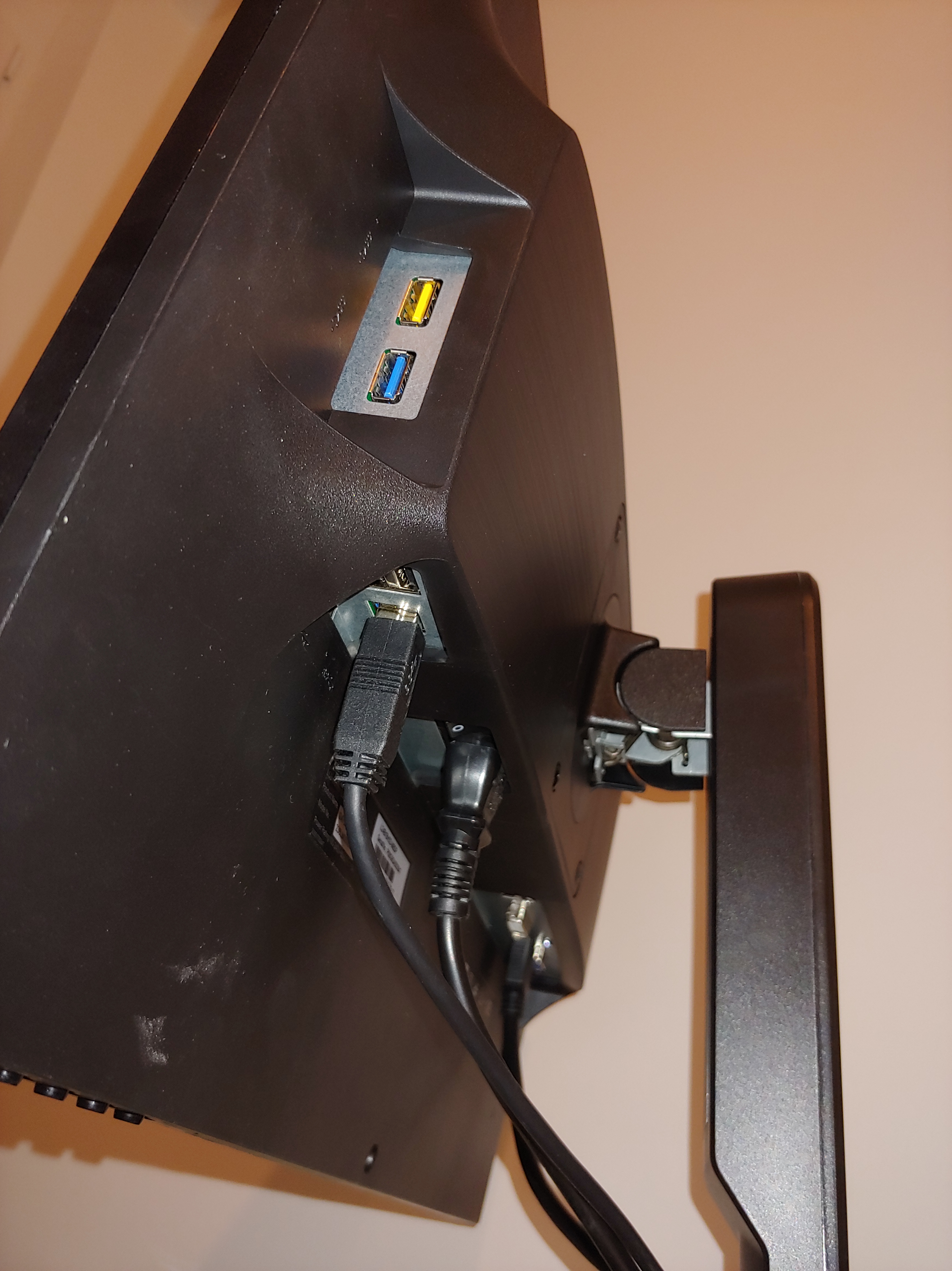
I was using the blue 3.0 port, which can provide up to 900mA of current, in theory. I shorted the output and it died. Also after a reboot and restart of the monitor: no self restoring protection. It was time to tearing it apart and I would exploit this fixing attempt to see a bit of what’s inside.
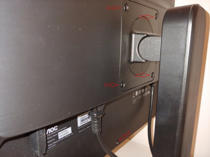
The monitor can be opened from the back, unscrewing these 5 screws.
At the bottom AOC made a nice cut to insert my favourite iFixit plier. I was tired to break my guitar pick ups.
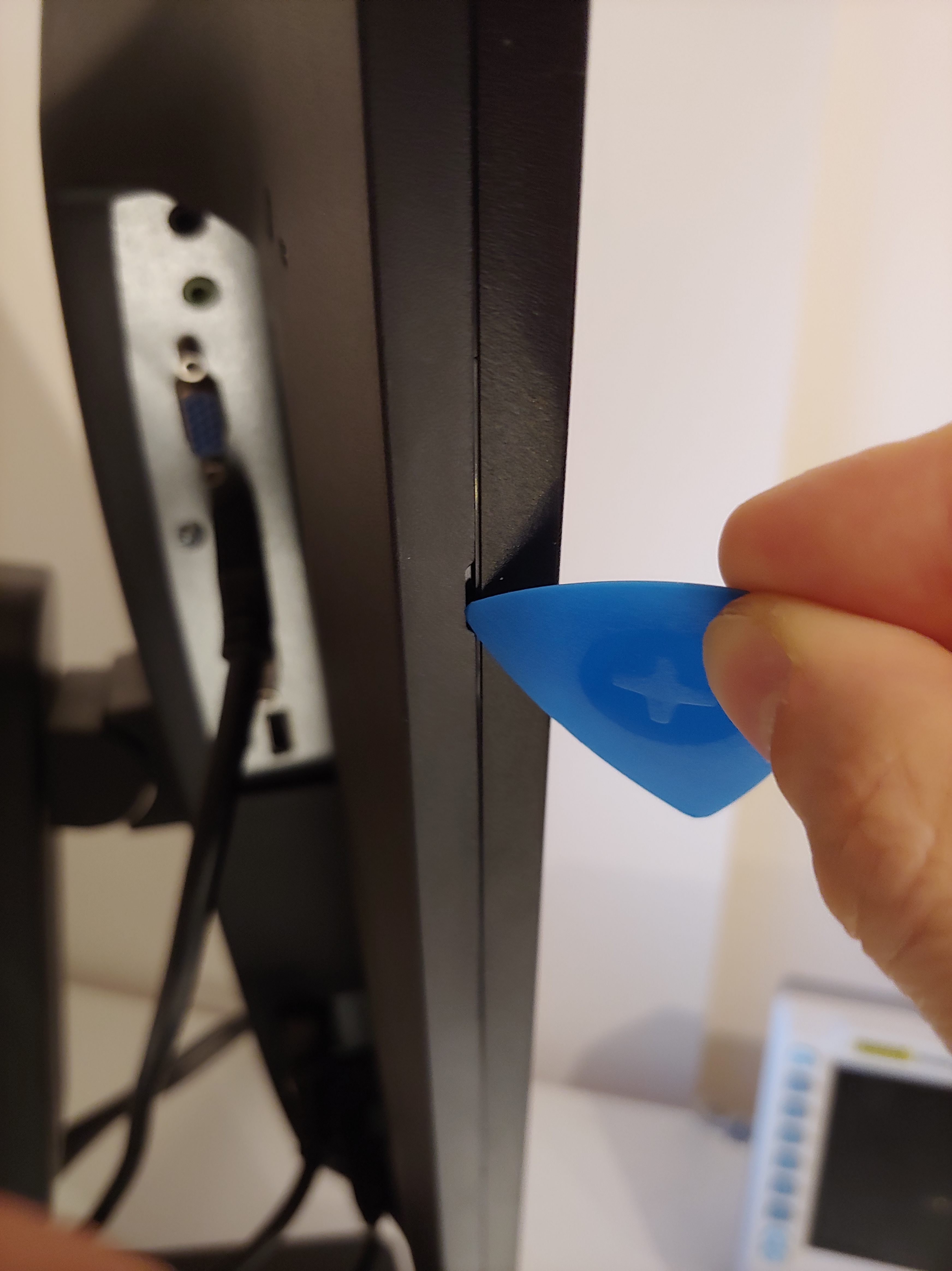
Inserting in it as per Figure 3 and gently sliding on all edges, the back cover pop out nicely showing the first inner parts.
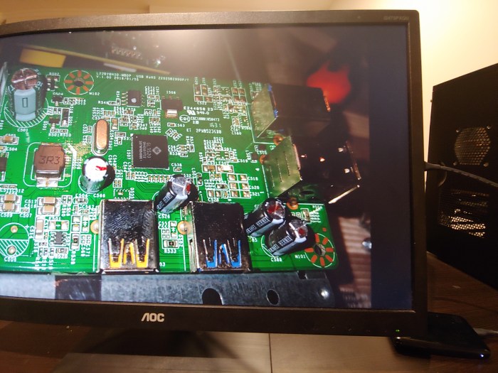
A look to the inner construction, or procrastinating the repair in name of curiosity
At the bottom of Figure 4, under the black tape, there the circuitry responsible to take the LVDS signals and transform them in a useful data to drive the lcd pixels. In Figure 5 I exposed it: it can be seen the LVDS PCB traces, at least 10 of them (so 20 traces). These are going into the Novatek NT71263FG, in the big red rectangle.

The interface in Figure 5 is made with 2 pairs of 4 bit differential signals: E3P and E3N, E2P and E2N, E1P and E1N, E0P and E0N for the first 4 bits. And O3P and O3N, O2P and O2N, O1P and O1N, O0P and O0N for the last 4 bits. Plus their respective clock. This is how I can tell is a LVDS signalling, with even (E) and odd (O) pixel data stream. The color data is at least 6bit per color in this monitor (but I read of LVDS FPD-Link using 7 bits, somewhere), so having potential to transmit from 18bit to 24bit of color depth, the serial transmission with 4bit of parallelism shown here suggests a 8bit transmission per 2 clock cycles/edges spread among these wires. This was checked against the LQ150X1LG82 datasheet and the “AN-1032:An Introductionto FPD-Link” and other documents. But I was not able to find any public information on the Novatek part.

The left highlight red rectangle (still in Figure 5) contains a low-dropout LD1117, probably for the Novatek chip itself and/or the Chipone ICN9101A, a datasheet-less part, close to the LDO and highlighted in Figure 6 below.

Considering some of 3 transistors on the pins of this Chipone part, a trimming pot and many “VOFF” test points, I guess is some voltage regulator for the bias of LCD pixels to provide the LCD drivers with the correct voltages, presumably in a configuration of a switching converter in the input and some internal LDOs in the Chipone part. But after finding the sell-sheet (in Chinese), seems to be a power manamgement IC for the TFT gate control voltages.
Then an IC205 in the RefDes of the PCB in Figure 7, corresponding to the ICN7211 (Chipone part), looking on their website, seems a Vcom buffer for the TFT.

At the end of the PCB in Figure 8 below, I see couple of ICN7209. No data found on them.
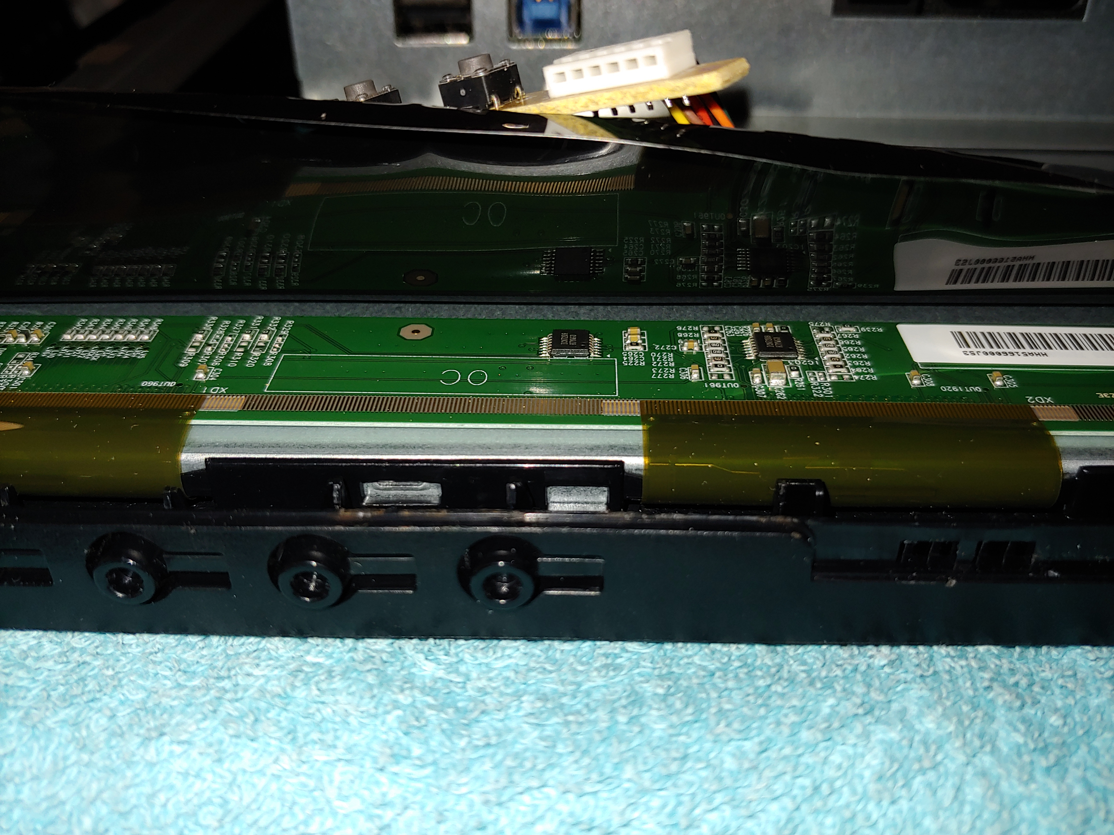
Continuing the disassembly, I am finally in the back of the panel, with a metal case and conductive tape keeping all together – Figure 9. To access the USB compartment, I need to remove such case. Interesting are the 3 thermal pudding attached to the metal chassis of the TFT panel to suck heat from the power supply board.

From left to right: the USB hub, the power supply and the monitor controller.
The main controller in Figure 10 really only consist of the integrated standard ASIC to generate the LVDS signals from the DVI, HDMI, DP or VGA ports. It also controls the audio from the DP or HDMI and send it to a dedicated audio chip. The rest of the components are 3 small EEPROM for identification when connecting to the PC with the 3 interfaces and couple of linear regulators.
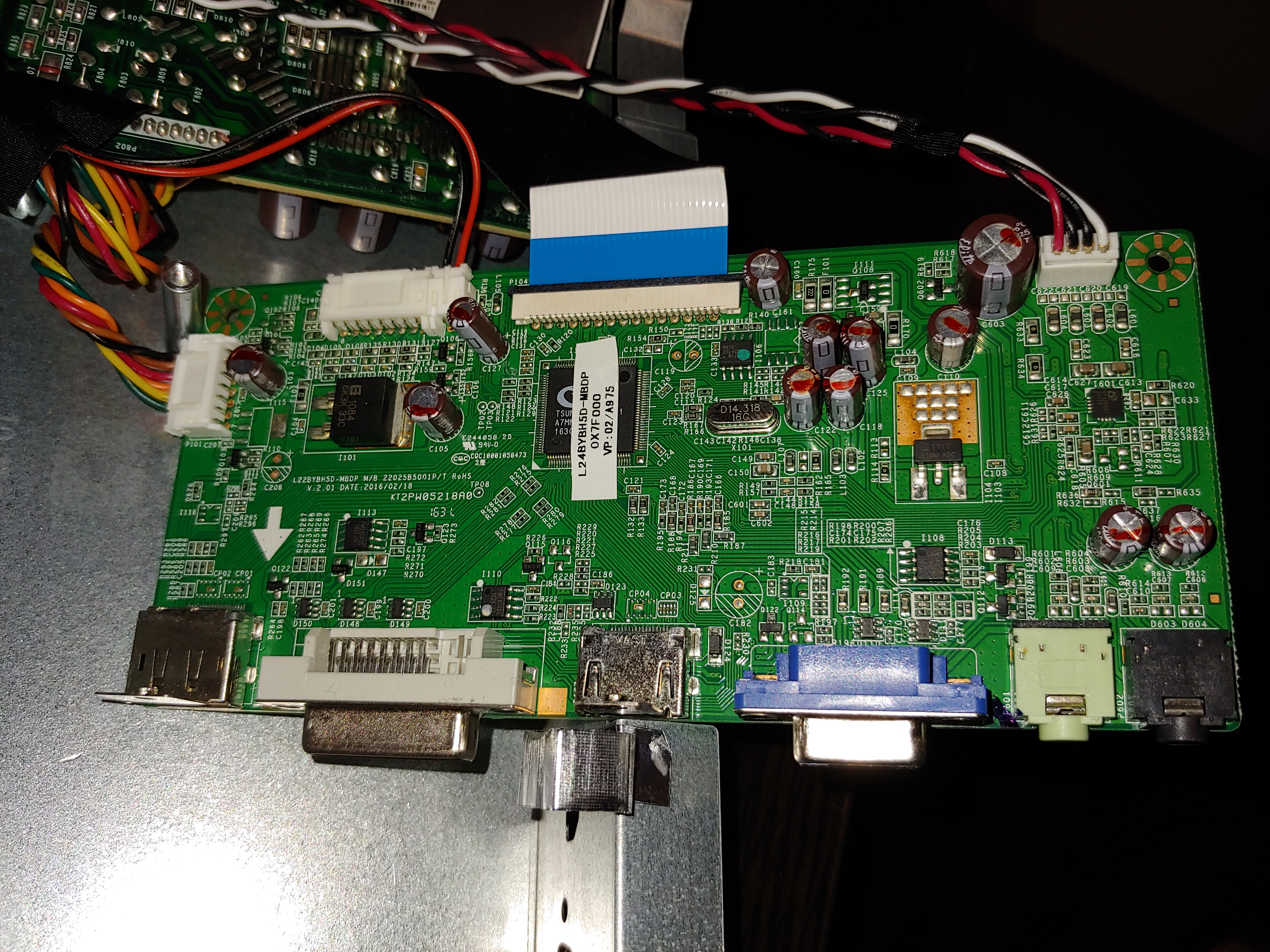
Taking a look on the audio chip, is a APA2604C, a 3W (into 4Ω load) Class-D power amplifier and headphones Class-AB driver.
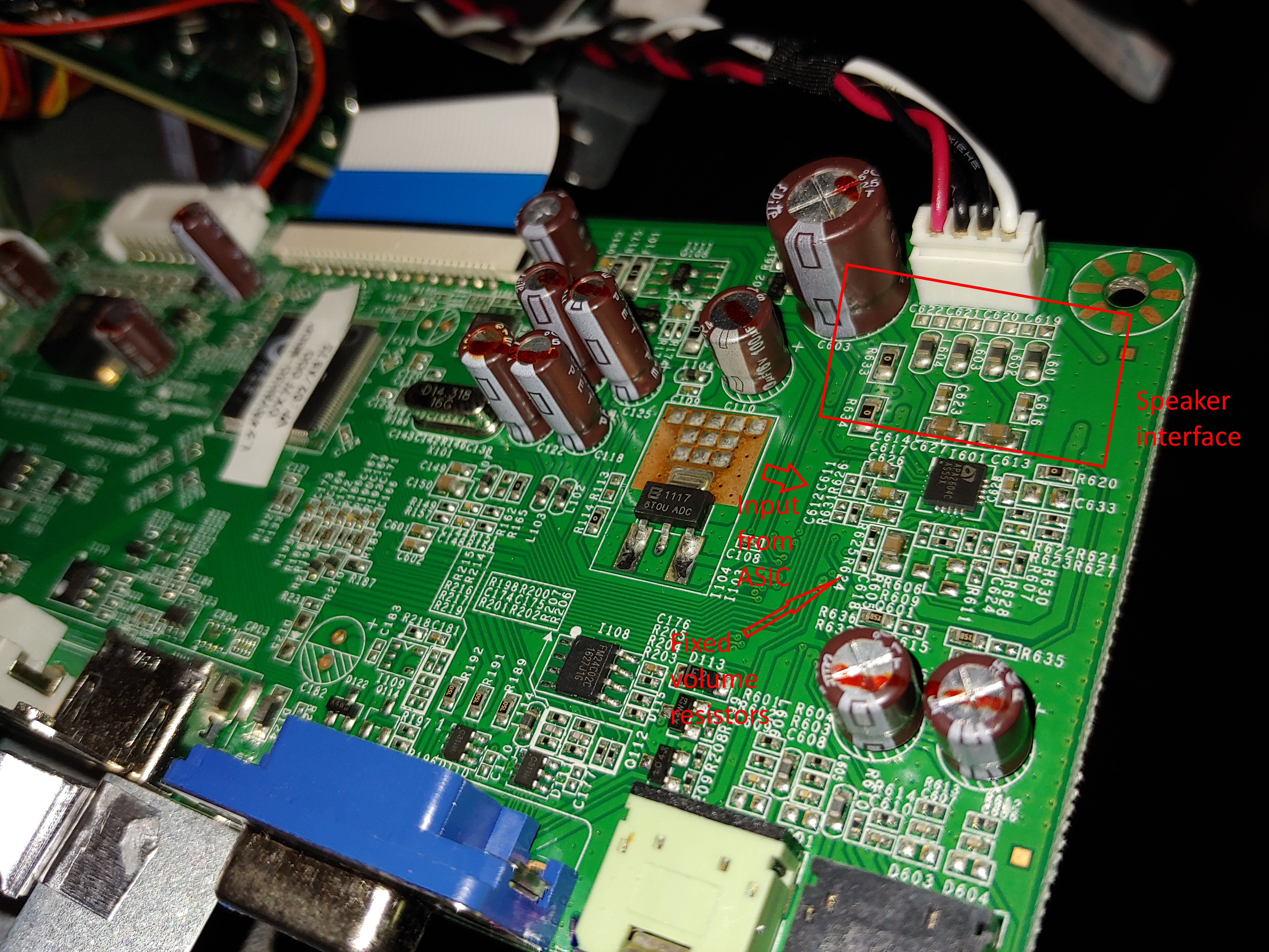
Volume and inputs are analog: the display controller adjust the volume by changing the amplitude of the input, because the volume of the chip is fixed with a resistor divider and a filtering capacitor on this divider. I did not proble the analog inputs, but I believe is a continuous analog signal pre-processed by some sort of DAC integrated in the main controller, because is fed through a resistor and a (non-soldered) capacitor while the audio IC can take analog input only. The capacitor on the inputs (i.e. C626 and C617) are instead DC blocking capacitors. Because of symmetric traces and the pin position, the layout of the speakers interface can be spotted too.
Now, coming to the power supply showin in Figure 12 below. One side of it contains the typical off-line SMPS power supply: fuse, varistor, common mode choke filter, rectfiyer diodes probably under the heatsink with the transformer driving transistor – all grouped in the section #1. All goes to the big smoothing capacitor, while the small circuitry close to the optocoupler IC will probably supply the SMPS controller (see section #2). Still in #2, we can find the HF transformer, EMC safety capacitor (HAS TO BE A SAFETY ONE, result is a dangerous power supply which can shock the user – there is a capacitor between us and death). Interestingly, such safety capacitor has a small ferrite choke on the pin into the low-voltage side.
Under the heatsink presumably the driving transistor of the transformers’ coils and an optocoupler. The section #3 contains the reservoir capacitors for the outputs and a output filter inductor. On the lower part of #3 there are 2 fuses, one per voltage rail. The six diodes seems a bit too much, maybe in parallel? What about a possible thermal runaway of such diodes? Maybe that is why are kept well far from the PCB, to keep them cool. The output channels with the inductor most likely is the one providing the cleanest 5V (or 3.3V) output and providing the feedback to the optocoupler. The higher 12V channel will rely just on the windings of the transformer, following the 5V regulation: it is a typical regulation scheme used on off-line SMPS multi-rails power supplies.
Lastly, the section #4 contains some of the basic components of a secondary DC-DC switching converter: a input capacitor, inductor, diode and 2 output capacitors.
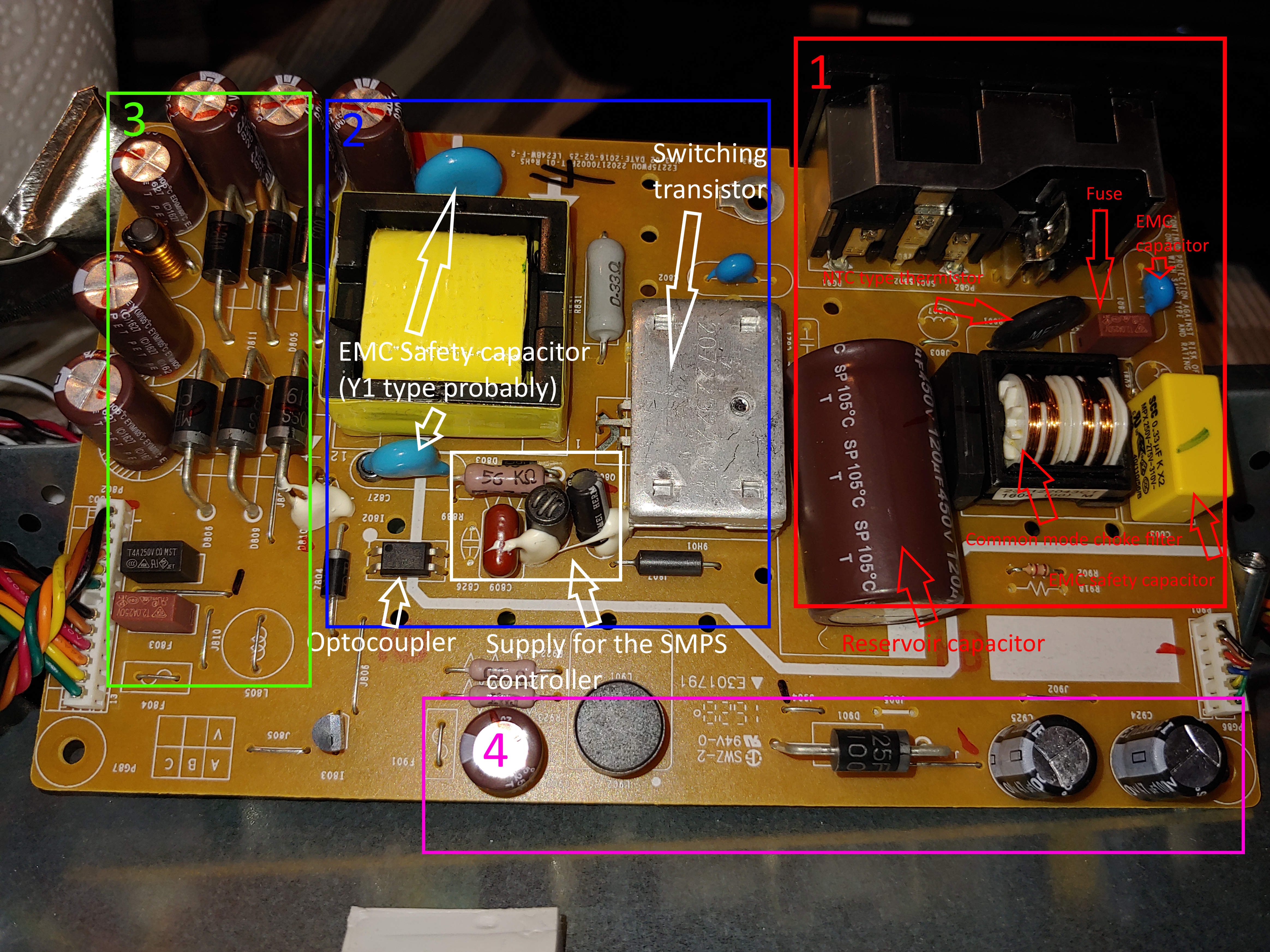
In the Figure 13 below, on the back of the power supply, shows the rectangles on the Silk layer of the PCB, where the thermal “pudding” has to touch. It seem they need to spread the heat of the HF transformer and the some resistors (3 of them in parallel, 100Ω each, see section #1), and at the beginning I believed they were in series to the diodes, as a technique to avoid thermal run away. But because this AOC is just a commercial cheap monitor, more realistically are probably for EMI reasons or to make a snubber network, since later I spot them to be in series to a small capacitor on the other side of the PCB. I think the thermal pudding keeping the PCB and the lead of the diodes cool, contributes to reduce the thermal runaway chance – so is an issue might be ignored here.
The section #2 probably contains the IC switching controller, because this SOT6 has connections to the optocoupler and receives power from the supply circuitry on the other side. The section #3 is the other PCB side of a secondary switching converter (#4 in Figure 12): it is insulated from the primary side, and there is a transistor switch and a SOIC-14 controller chip, a OB3351CP part.

I noticed how the backlight is finely controlled, with no flicker at all (as advertised by AOC): it must have some sort of special analog circuitry. Turns out the OB3351CP part is the controller chip for the backlight. On line I have only found similar parts, like the OB3350, which seems to be a switching LED driver for LCDs. The 2 output capacitors of section #4 are suggesting a DC output, adjusting finely the output voltage to keep the required LED current.
The actual repair
Finally coming to the culprit, the USB hub. Is made by using the somehow widely used GL3520, a little bit more documented part than others found so far. Is an 8-bit MCU including all the PHY layer of the USB 3.1 and implementing the hub capability. What I am interested is to find why one 3.0 (well, 3.1) port stop to provide power – which is the reason of all such teardown.

Probing around, looking in Figure 14, seems that the power USB (yellow) uses the 5V from the on board regulator in section #1, which takes the 12V from the power supply previously seen in Figure 12 and 13. The section #3 contains the main controller IC, the serial flash for the controller itself and a local LDO. What is interesting is the Fuse which seem to be blown.
So I decided to put a PTC, rated at 600mA at 25 °C (and also because luckily was already available in my component box. Because is a USB 3.0, with a delivery capability of 900mA, I decided to put two of them in parallel. Not the best idea, but with few tests I shown to myself a tripping current of about 1A, despite the voltage was dropping down to 4.7V or so, where the standard ask for a 5% tolerance, resulting in 4.75V minimum.
Here a tripping event from the scope when the circuit was loaded and unloaded:
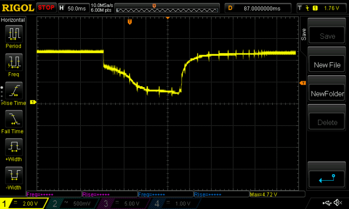

Fair enough to guarantee some sort of protection. The spikes are coming from the supply of the hub, probably from the converter in the section #1 in Figure 14, since it seems a waveform of a hiccup current protection of the converter itself.The hub was tested without connection to a PC, but was just powered from the monitor itself. Good idea? We like living on the edge!
While below is the output of the yellow power USB, which provides an electronic protection shown in section #2 of Figure 14. Is more clean, suggesting the IC close to that port is actually doing something without further investigation.

The trials must be done in a small number, because the PTC degrades each time trips. With a sustained load of 1A, trips only with an ambient temperature a bit higher than 25°C, so no much precision is expected, typical of PTC protection. And the output voltage at 1A degrades to a 4.5V because of the PTC resistance. Now I know why they used a non resettable fuse: no drop happens and USB voltage compliance is granted. Using my power hungry USB hard drive and my fidelity USB monitor, when the hard drive reach 600mA, the USB voltage drops to 4.7V which is 5mV below the allowed value by the standard. For not big power hungry devices, is perfectly fine and better than a non working port and the hard drive did not shown any symptom – if that could matter.
Interestingly, while measuring the other 2 USB 2.0 ports, I blown also their shared fuse, the F503 in the Figure 18. So I exchanged also that one. In Figure 18 is also shown the new PTC compared to the old one.
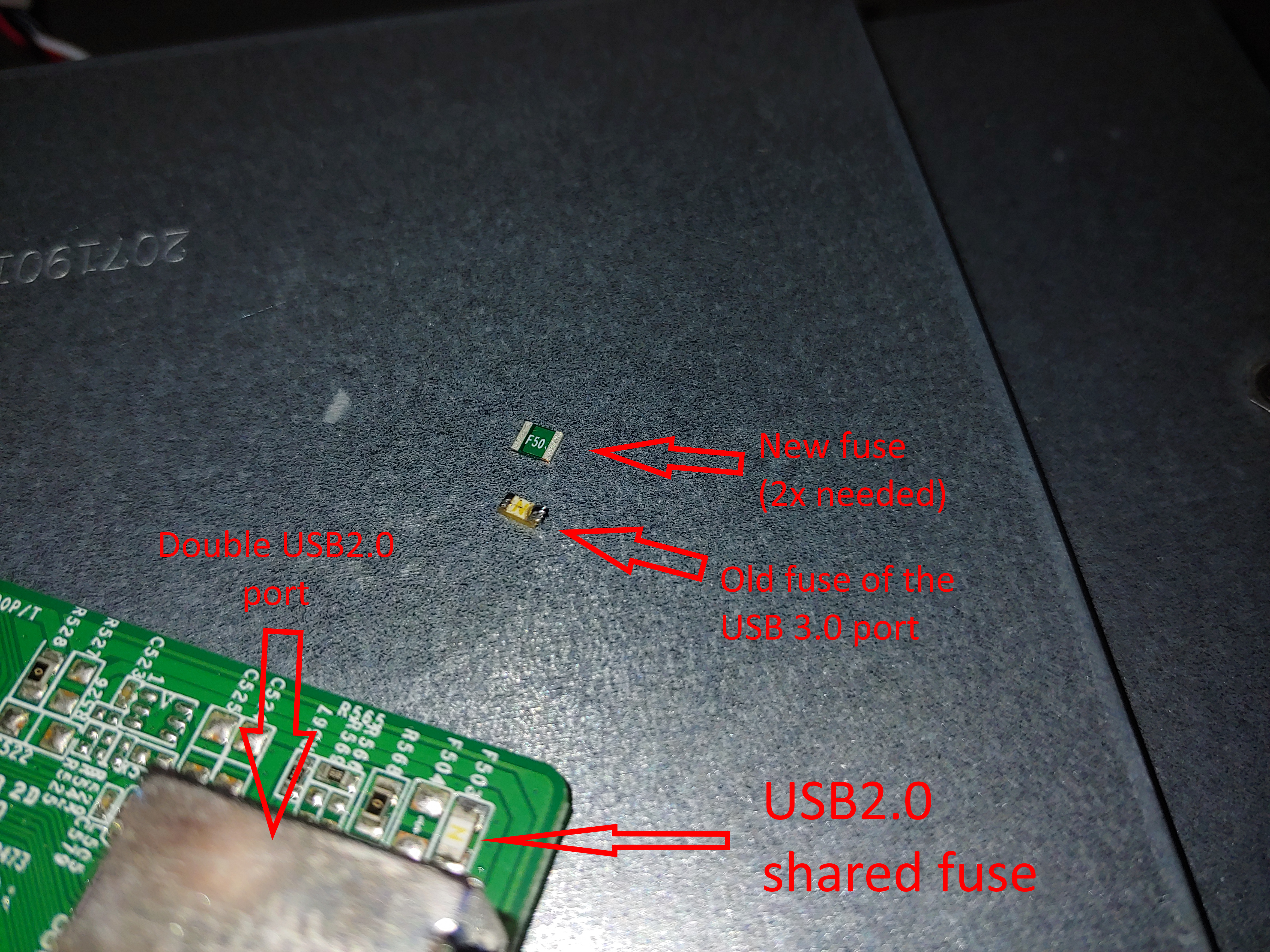
And here the final fuses soldered.

And luckily assembly back the monitor went fine as well.