
I started to experiment with the WS2812 LED, more specifically the WS2812B, which is a better revision in term of connections. These are the very famous individually addressable RGB LED, where tons of sources are available. Mainly due to their low cost, they are spread to the maker scene like a rhinovirus in a primary school in February.
And here I am, writing about this little adventure because I personally learned a lot from it and someone might benefit as well. Also, I discovered something interesting about stretching this WS2812B protocol, additionally on what is mentioned in the cpldcpu.wordpress.com article which inspired mine – and I really suggest to read it to learn on how to think when reverse engineering a simple protocol.
So back to us, the plan is to set up some basic firmware (actually, a bunch of instructions) and make an hello world with this LED. The device uses a clockless communication, with the bit encoded in a PWM signal, with apparently tight speed requirements:

Those timing are shown in the datasheet’s table:

That means, between a 1 and a 0 is needed a resolution capable to withstand a Δt = T1H – T0H (see Figure 1, red marking), that is 0.4us with a tolerance of +/- 0.15us. With the tolerances in a worst case scenario, reducing the difference of T1H – T0H, this goes down to a 0.1us of resolution. Something is wispering that is not going to be trivial. And I thought it was just a silly RGB LED. Actually, a GRB LED.
A nice way to overload the CPU and not driving the LED
If I encode this with an output compare or PWM, I have to consider the speed of the updating period. With the tolerances shortening the bit period of 150ns for the high and low levels on the waveform, the total period is shortened of 300ns, which means the nominal 800kHz will rise to 1.05MHz. On the other hand, a longer period will increase of 300ns lowering the speed to 645kHz. Apparently there is some room for speed adjusting. Then, since I have no DMA in this small 8-bit MCU, I can only update the data in a ISR.
Ideally, we should setup 800kHz PWM frequency, or 1.25us of period. With the Atmega328P I can set the PWM period, with no prescaler, down to the CPU frequency (here 16MHz) divided by the PWM frequency, 

This means that after TCNT0 count up to 20, at 16MHz speed, will be elapsed 1.25us, i.e. the OC0B pin will provide a period of 800kHz. We just need to trigger the ISR after TCNT0 = 20, update the duty cycle register and voila! Right? Well..
The reality is more like the following:

In Figure 4, after the counter reaches the maximum in 1.25us, the ISR needs to fire. There are all the PUSH instructions to the stack, each of them taking 2 clock cycles. Plus all the execution inside and the return of the ISR, RETI (which takes 4 clock cycles), must be added to the POP instructions. To stay in time, is almost impossible. Here the C part of the ISR (complete code at the end of the article):
ISR(TIMER0_OVF_vect)
{
	TCCR0B &= ~((1 << CS00) | (1 << CS01) | (1 << CS02)); // stop timer
	TCNT0 = 0; // reset timer
	OCR0B = serial_data[bit_counter++]; // update dc
	if (bit_counter <= 50)
		TCCR0B |= 1;
}
While the disassembly is:
00000051  PUSH R1		Push register on stack
00000052  PUSH R0		Push register on stack
00000053  IN R0,0x3F		In from I/O location
00000054  PUSH R0		Push register on stack
00000055  CLR R1		Clear Register
00000056  PUSH R24		Push register on stack
00000057  PUSH R30		Push register on stack
00000058  PUSH R31		Push register on stack
	TCCR0B &= ~((1 << CS00) | (1 << CS01) | (1 << CS02)); // stop timer
00000059  IN R24,0x25		In from I/O location
0000005A  ANDI R24,0xF8		Logical AND with immediate
0000005B  OUT 0x25,R24		Out to I/O location
	TCNT0 = 0; // reset timer
0000005C  OUT 0x26,R1		Out to I/O location
	OCR0B = serial_data[bit_counter++]; // update dc
0000005D  LDS R30,0x0104		Load direct from data space
0000005F  LDI R24,0x01		Load immediate
00000060  ADD R24,R30		Add without carry
00000061  STS 0x0104,R24		Store direct to data space
00000063  LDI R31,0x00		Load immediate
00000064  SUBI R30,0xF6		Subtract immediate
00000065  SBCI R31,0xFE		Subtract immediate with carry
00000066  LDD R24,Z+0		Load indirect with displacement
00000067  OUT 0x28,R24		Out to I/O location
	if (bit_counter <= 50)
00000068  LDS R24,0x0104		Load direct from data space
0000006A  CPI R24,0x33		Compare with immediate
0000006B  BRCC PC+0x04		Branch if carry cleared
		TCCR0B |= 1;
0000006C  IN R24,0x25		In from I/O location
0000006D  ORI R24,0x01		Logical OR with immediate
0000006E  OUT 0x25,R24		Out to I/O location
0000006F  POP R31		Pop register from stack
00000070  POP R30		Pop register from stack
00000071  POP R24		Pop register from stack
00000072  POP R0		Pop register from stack
00000073  OUT 0x3F,R0		Out to I/O location
00000074  POP R0		Pop register from stack
00000075  POP R1		Pop register from stack
00000076  RETI 		Interrupt return
When double buffering is not your friend
Optimization is useless, we are way beyond the 20 clock cycles. Just the 6 pairs of PUSH and POP are taking 24 clock cycles, plus everything else – meaning the timer wraps more than once when the ISR executes, see diassembly listed before. So, I expect to see the timer firing and waiting a long time or something weird to happen. Probing, I see this (well, the green comments were not made by the scope):
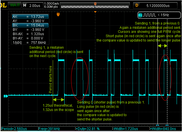
Considering just the ISR overhead lasting more than the timer period, the acquisition in Figure 5 become less misterious. After sending the first “1” with a duty cycle long ~800ns, the ISR executes. Then the timer is stopped, reset and the OCR0B register updated. But because the timer wraps before updating the new value, it will issue at least one more PWM cycle with the old duty cycle. Also, in fast PWM mode the OCR registers are double buffered and new value is applied after wrapping over from TOP to BOTTOM, meaning that updating the new compare value after the timer started, will output the previous buffered data. Hence why we not only see one pulse more, but when updating the new one, the old appears once before in the spurious pulse (as shown in the red circles). This has to be taken into account when handling the number of ISR which has to fire to send the data.
If the WS28xx pixels are cheap, it must also be the design of the control for every pixel. AKA how to successfully trick the pixel to work properly.
The table in Figure 2 states that a reset/apply command on the LED is issues when keeping the signal low for more than 50us. But if this is true, then what happen between the T0L and Treset time? Did they implemented a more complex FSM which filter out timings in between? According to Cpldcpu article and common sense, the FSM is very simple. It just count the samples and makes a discrimination between a 1 or a 0, and if the counting goes too long, it will be a reset, otherwise it will accumulate the last bit in the shift register at the next rising edge. Duration is estimated according to a local RC oscillator. It does not really make sense to implement a “dead” area detection mechanism in which errors might arise or signals ignored without a reset. Also, the pixel is different, as now have all the 3 dies are on the same lead frame:

EDIT: the new WS2812B datasheet states 280us of reset duration, to allow firmware written for weak&cheap MCUs also control such LEDs. Thinking about it, there would be no much sense in saving on LEDs if I need to code with complex 32-bit CPUs.

To prove that slower timings are fine, I increased the PWM period from 1.25us to 16us, which is still well less than 50us, hence having the TCNT0 counting up to 255 instead of 20. The pulse is shaped to last ~800 or ~400ns. With the PWM inverted, the high bit pulse will set the pin high from 242 to 255, while the low bit pulse will start from 249, making a shorter one. Essentially the resolution is 62.5ns, which is one clock cycle duration.
Differently from other tests done in the Cpldcpu article, the LED seems to accept the longer low level. That’s compatible with the new datasheet (at time of writing is Ver. 5). Also correct data is output reashaped for the next LED, shown by cascading LEDs:

Also, the CPU seems to have more time, as I sistematically get, in debug, a TCNT0 value of 24 after stopping it, so I assume it does not wrap. In fact, there are no more than 34 clock cycles between starting the timer and stopping it again. This means that before reaching the value 242 and hence creating a second pulse, there are other 242-34 = 208 clock cycles, or 13us at 16MHz, available for other code to execute – possibly not in a ISR to avoid race conditions or timer wraps, while the WS2812B transaction is happening. This means that despite the CPU is quite busy during the transaction, is still not fully occupied looping in ISR calls and does not stuck completely the rest of the code.
This is the whole code, sending two color samples. A video shows the result of the test:
Are there any conclusions?
In the end I just wanted to light up some LEDs. But I learned few more things, for example:
- Double buffered registers for the PWM are generating a latency of one sample which has to be taken into account or at least one must be very aware of the mechanism
- The WS2812 datasheet is written in proper Chinglish
- The communication protocol seems to be simpler than what is stated in the datasheet, making room for some “abusing” or workarounds
- The pixel seems to have loose timings, with a reset of 280us. Is proven to ignore the reset with low pulses of ~20us, allowing the workaround to take place.
- Learned almost by heart the execution time of the main AVR assembly instructions.
