
When I needed to design a dual power supply I was looking for parts capable to handle buck, buck-boost, with inverting and non inverting properties. Because I was also looking for a contained budget, I’ve been fascinated by a single, multipurpose part, capable of doing all of this. I immediately realized it was the 555 equivalent of DC-DC converters: the MC34063.
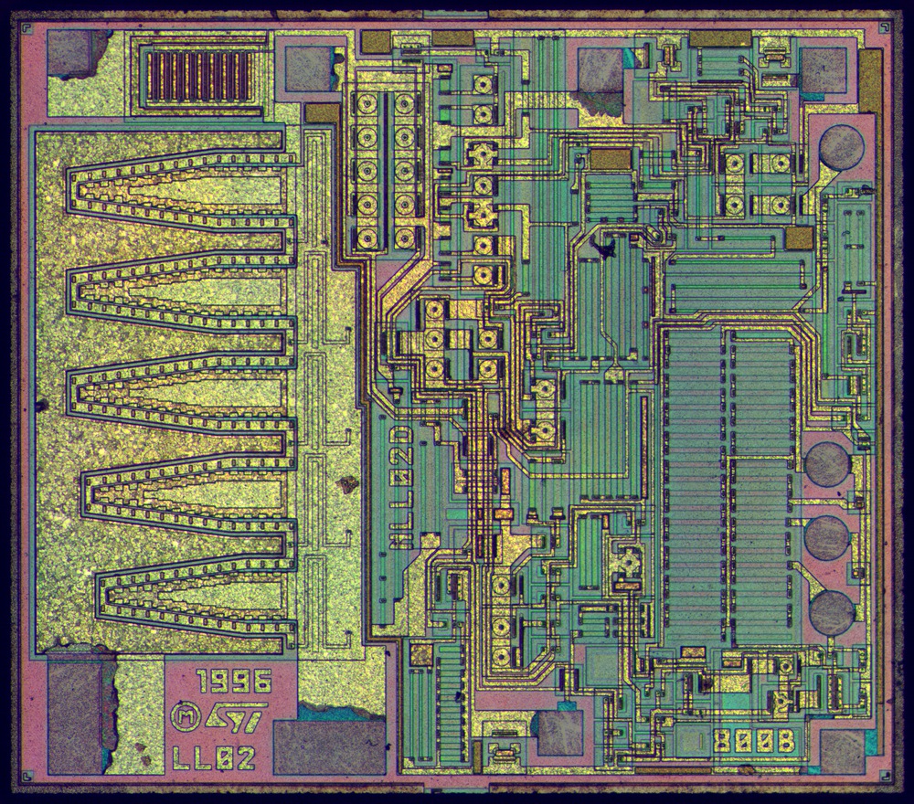
For who has some difficulties in spotting the circuit from a silicon layout:
The key components of switching regulator that do not necessarily need resize if the project changes, are a control signal for a switch, a comparator, a reference, some sort of time keeping (active or as a result of the natural time constant of the circuit). Plus diodes, inductors capacitors and the like to interface with such components. The MC34063 offers most of these parts, and pin connections can be re-arranged in different ways to achieve any switching supply configuration. In this article, I’ll go through the design of the inverting configuration. In the next article, I will show the final circuit working.
Basic equations of the inverting example
A way to start is to think how we could invert the output. It has to be a current flowing in a reversed way with respect to the source. With a bit of immagination, we need to keep the current flowing always in a opposite direction to achieve a negative voltage. We know an inductor can somehow be used to keep a constant current, for example. It must be loaded to induce it (is an inductor after all) to let current flow in one direction, and then keep such current “momentum” and applying it to the load.
As a result, the literature (and our pen and paper creativity) provides us with something like this:

When the MOSFET switch S closes, the input voltage is onto the inductor, for a given duration here we call 


To start a basic analysis, let’s keept the inductor’s equation at hand:

At time ton, 


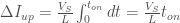
So is possible to get the increase in current during
At time toff from the same inductor equation 1, during 


In the same way, integrating over duration

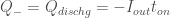
At steady state the average current must be constant, hence all the increase in the current should be followed by a negative increase, hence why, from eq. (5), 

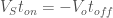
Equalizing eq. (3) and (5) we get:
Hence:

Note that here the average current of the inductor does not matter, but only its variation. We will see later, both in words and formulas, how the peak inductor current will determine not the output voltage, but the output average current.
Learning the system more deeply through a real design
Let’s start from some specification we want to achieve. Some of them are modified to be stretched on purpose to develop better a feeling of what might be wrong or not efficient:
- Input voltage: 4.5V to 9V
- Output voltage: -25V
- Output current: 10mA to 100mA
- Inductor current ripple: +/- 30%
- Output voltage ripple: +/- 1%
- Switching frequency: 50 kHz
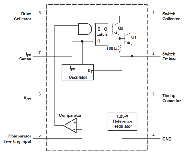
For the diode, is assumed to have a forward voltage of Vf = 0.4V. In the configuration of Figure 3, the IC is configured as follow:
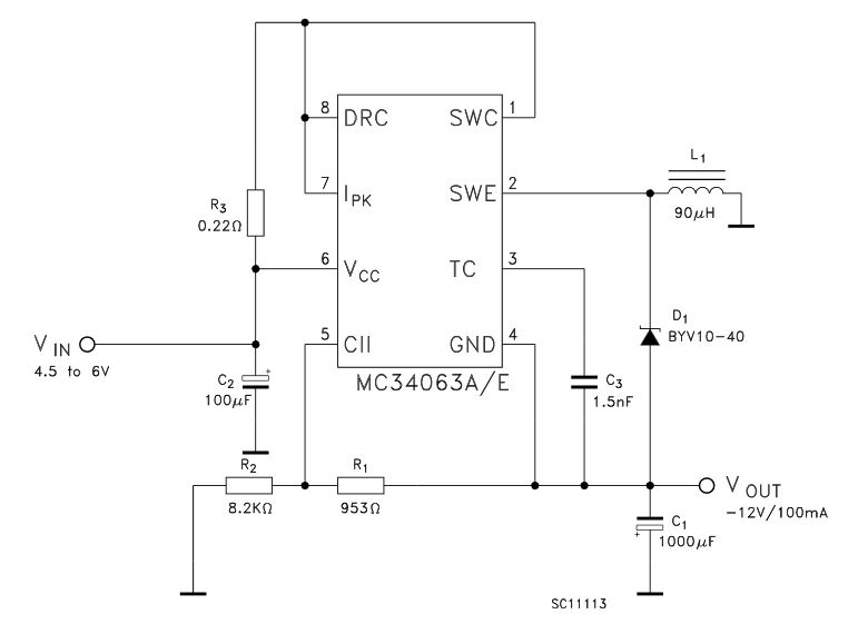
With this configuration, the integrated transistor is emitter follower, and being a Darlington total saturation voltage the sum of the first BJT Vce (saturation) plus the output BJT base-emitter voltage, it reasonable to assume now that we are going to dissipate a lot. We can always verify that later. From the datasheet, its maximum is 
MC34063 specific: switching timings and frequency settings
Here is determined the value of the timing capacitor needed to set the frequency of the switcher. Here I describe the way how is done in the MC34063, so with another part will be completely different. Always read your datasheet!
Now from clarity let’s call the 


With a switching frequency of 50kHz we have:
and extracting

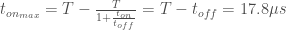
So that the important time parameter, the maximum
According to the minimum input voltage, as we will see later, this timing will determine the maximum inductor current.
Specifically referring to the MC34063 part, timing is generated by a voltage ramp in an analog counter inside, but at the end of such ramp, it takes a 1/6 of the time T in order to reset the counter and start again. So we can expect the frequency to be a little lower. Note: here I am referring to the small signals of the timing capacitor generated from the oscillator block in the chip, and has nothing to do with the output capacitor or the output current.
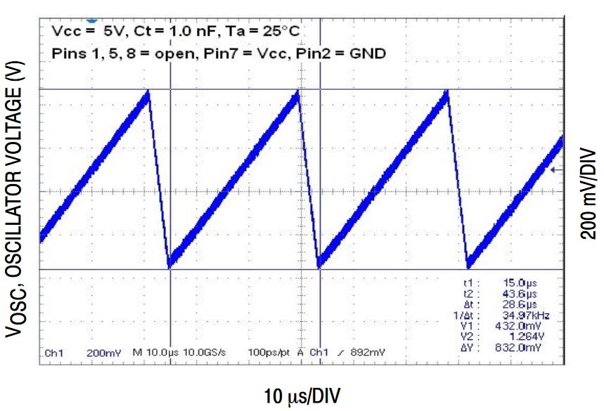
When we choose a period, we are in fact selecting the slope of the voltage on the pin 3, where we put a capacitor CT with a constant small current generated inside the integrated circuit. Note that the up and down slopes together are forming the period T, but during the down slope the output switch will be turned off: we cannot have the 100% of duty cycle – a typical characteristics of many converters, up to use the advertisement of a “truly” 100% duty cycle in parts which are addressing this issue.
Therefore the maximum duration of the rising current represents the maximum ton period, useful later as we will see. Back to the timing capacitor, its equation is 
But since from Figure 5 we have the 
From the datasheet, typical Ict = 33 uA, and from Figure 5 (still taken from the datasheet), 

Normally in the design process one would normally only takethe equation (10a), which is provided inthe datasheet, but personally I wanted to understand from where such a constant was coming from.
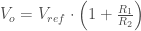
MC34063 specific: feedback voltage
The MC34063 needs to fed back the output voltage and downscaling to an internal reference of 1.25V. This is usuallt done with a voltage divider, for which the accuracy of its resistors, as well as teh reference, are defining the output accuracy. Such accuracy is worsened by the ripple, step in the current absorbed by the load ecc, but is a good indicator of what to expect in the output. I left out the accuracy from the requirements as it doesn’t really matter if I can adjust with a potentiometer. But for semplicity, I will just go with a normal pair of resistors as in Figure 4. Later improvements can be done.
From Figure 4, the pin CII shall be regulated to be the same as the reference Vref and therefore:

So that the output is:
There are couple of ideas when choosing the resistors: either making them small enough to have the minimum load applied through them, or we want low power consumption with no load, so R1 and R2 shall be very big, but not so much as the feedback current has to be much bigger than the bias current of the comparator, which is up to 400nA, So we can neglect the current flowing into the comparator inputs. We can choose 500 uA, as 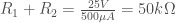
From eq. (11a) we find:
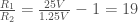
Solving for R1 we have:

But as we assumed a total resistance of 
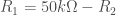

Finding 

Any adjustment can be done during the protoyping phase.
Dimensioning the inductor
From the Figure 3, the sum of currents at the node connecting the capacitor C, the load and the diode D, is 

And can be seen by the following graphs, at “Capacitor 
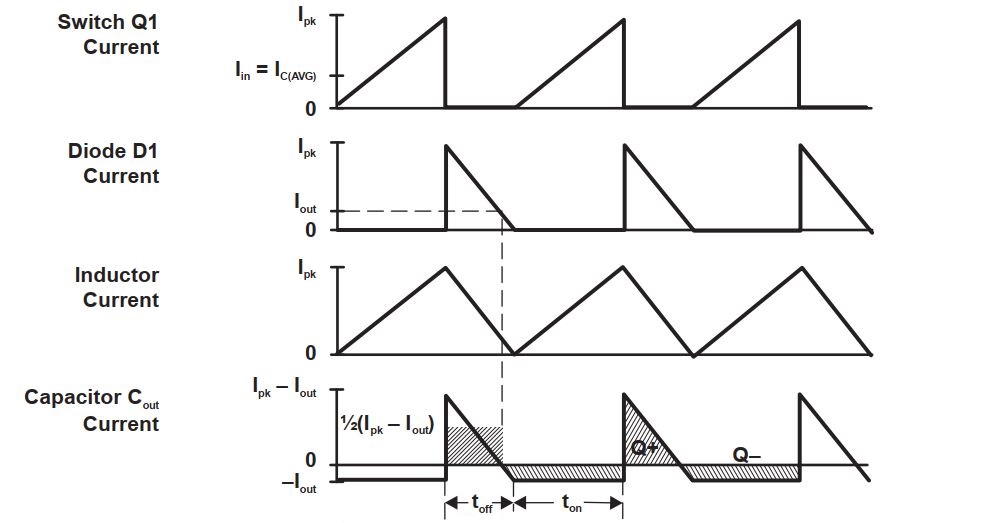
Durigh both 
From these waveforms we see that the inductor current is made by 2 triangle, each representing the rising and falling current of the inductor. It is not connected to the load or the capacitor current when charging: this separation of currents characterize the boost and buck-boost architectures, leading to a different peak current calculation when compared to the buck. Paying attention to Figure 6, the capacitor gets charged during almost all
But how can we define the inductor current 


The charge will be:

Note that the result in eq. (13) is the area under the capacitor current in Figure 6. During 

And during the whole period the total charge should be 0 to have the voltage contant, hence:

Substituting eq. (14a) and (14b) into eq. (15) and solving for Ipk, we get:

Now, too many different application notes and datasheets are freely using mixed definitions for the duty cycle D and its off-duty cycle 1-D, so here my golden reference:

So that the eq. (16) can be rewritten as:
The form in eq. (17) compared to eq. (16) is quite important, because from the eq. (8) representing the input and output voltage relation, we can see how the output voltage and input voltage are defining the peak current.
From this observation, I like to see also intuitively (with no math) why a DC-DC converter transfer to the output the same amount of power. Absorbed current will be inversely proportional to the input voltage, in order to transfer the same input power to the output, ideally. A ramp that exists for longer time, within the switching period, results in a higher average input current. So with a lower voltage, the slope is shallow and the converter will extend the on-time allowing the overall energy to be the same. Hence why, lower the voltage, higher the current to keep the same amount of power taken from the source, but within the switching period boundaries. The magic is all about having the “converter will extend” part working fine.
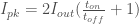
The peak inductor current is also an important parameter when choosing the inductor and the voltage ranges. Therefore the peak current will be, based on the initial worst case requirements:

And is not a very small current.
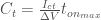
We can now find the minimum inductor value required to withstand the peak current requirement just found. Again, from inductor equation (1), integrated over the maximum period ton, we get:

And from figure 3 we know the voltage is constant and is VL = Vin – Vsat , meaning we already include the BJT’s saturation voltage. Solving for L and substituting the definition of VL, we find the minimum inductance:
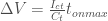
$latex L_{min} = \frac{V_{in}-V_{sat}}{I_{pk}} t_{on-max} = \frac{4.5V – 1.3V}{1.82A} 17.8 \mu s = 31.3 \mu H
But is not finished! To support the lowest output current without necessarily going in Discontinuous Mode, we must keep the inductor running at the end of the period T without getting it totally discharged, hence it must be bigger, with lower peak currents but also shallow slope in its current. We can think geometrically here, where a shallow slope over the same amount of time will reach a lower peak current. But with a big inductor, with the same voltage applied, results in a more gentle slope. Hence from specifications, we can apply eq. (17) with the minimum current:

And as a consequence the maximum inductor required to have the stability of the Continuous Mode is:

In the final design such big inductor can be used, but it would be pointless. With little power, the lower efficiency of a DCM would not play a big role. The result is that at lower currents and even higher that the minimum designed current of 10 mA, with a lower inductor (i.e. 330 uH), the slopes will be faster than the minimum on duration, hence the switch will be shutdown before the expiration time, up to when the sensed voltage will go below the set threshold.
MC34063 specific: short-circuit protection
This paragraph is going to be short. Like the short circuit feature of the MC34063. But here things might be a bit confusing, therefore I think is important to clarify that the comparator is not the feedback comparator, but the one in the oscillator, like in the following figure:
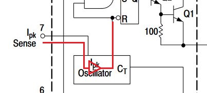
And the capacitor current is referred just to the timing capacitor and has nothing to do with the output capacitor of the regulator. Same for its current, where the constant current is generated inside the oscillator block, generates a trangle voltage waveform at the timing capacitor shown in the beginning in Figure 5.
When the output is not yet at steady state, the comparator will not turn off the switch before the ton-max period. But if the input voltage is big enough, at the ton-max instant the inductor current migh be higher than the peak. This might happen if one shorts the output, not allowing a correct feedback signal to be fed back. This applies also during the startup, hence is very important to limit the inductor current in any situation of the regulator. So the peak detection, or short circuit detection, is a comparator embedded in the oscillator with a reference of 300mV (again, see Figure 8).
Inserting a shunt like R3 in figure 4 (which we can call Rsc for short-circuit) and knowing the inductor peak current, we find:

When the shunt produces a voltage higher than 300mV, corresponding to an inductor current higher than the allowed peak, triggers a signal inside the oscillator, increasing the current of the timing capacitor found from eq. (10a), increasing the voltage slope of the timing capacitor shown in Figure 5, modifying it as the red mark in Figure 7, and anticipating the shut down of the transistor:

So from eq. (19) we find the short circuit resistor 
Output (and input) capacitor selection
During ton the diode is reversed biased, hence prevents the input current to disperse into the load, hence the load current will be exactly the output capacitor’s current. To quantify this capacitance, we can start like we did for the inductor, let’s consider the capacitor equation:

We know the maximum on-time, the maximum load current, and the voltage variation allowed, i.e. the ripple from the specifications. Such ripple is defined before to be +/- 1% of -25V, meaning -/+ 250mV (the reversal of +/- and -/+ is intentional). Solving for C in eq. (20) and putting the requirements in the known variables, we get:

The datasheet of the MC34063 suggests a value 9 times greater than this, so we can chose 
And what about the current in the capacitor? With a ripple from a triangular(ish) voltage, its RMS value is the peak devided by 

The capacitor impedance Zc is also combined with the series resistance ESR, so:

We know f = 50 kHz and Co = 33 uF, but the ESR will be defined when sourcing the capacitor, so the RMS current will be defined according to which part fits our requirements of low cost, for example. We just need to remember for now that 
So what will matter when looking for a suitable part is having a cost low enough to expect some ESR (if we choose an electrolytic type) and with that ESR and impedance we must check if the power dissipation is within limits. This will be done during the component selection, as at this design stage we still have no idea of what the market has to offer.
And the input capacitor?
The input capacitor instead has to be big enough to work as a tank reserve during the absorbed peaks of current, and mostly depends on the source which powers the converter itself. A 
Results achieved and next steps
From the initial idea to explore a jellybean part, we have made an idea on how complex its usage is. In the meantime we have brought up a design foundation for a buck-boost inverter. This was done by covering a bit the theory behind an inverting DC-DC converter, and applied this theory to find a correct dimensioning of the various external components. To finalize, we have found that we need the following components to achieve our theoretical design:
- Inductor L = 330uF
- Output capacitor Co = 33 uF
- Input capacitor Cin = 10 uF
- Timing capacitor Ct = 680 pF
- Diode with Vf = 0.4V
- R1 = 47.5kΩ; R2 = 2.49kΩ
- Rsc = 1.5Ω
But this is not enough to build an inverter. In fact, we still need to check the thermal capabilities of these components, to be sure we are not out of specifications, then source the various components from a seller, check if their dimensioning is realistic (i.e. does such a part exists without spending an arm and a leg?), bring up a layout and test the result. So in the next part I will go through the real components check and selection and then, the board layout. By then, we will discover if our calculations and deductions were correct! Stay tuned, like the feedback of a regulator!
